NCP5667 Description
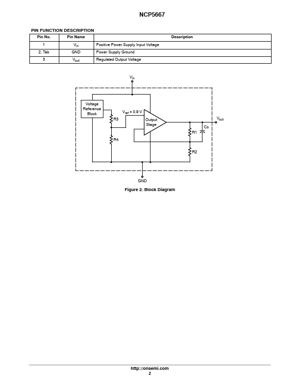
Pin Name 1 2, Tab Vin GND Positive Power Supply Input Voltage Power Supply Ground 3 Vout Regulated Output Voltage Description Vin Voltage Reference Block Vref = 0.9 V R3 Output Stage R4 Cc R1 Vout R2 GND Figure 2. Block Diagram http://onsemi. Maximum Ratings are stress ratings only.
NCP5667 Key Features
- ±1% Output Voltage Accuracy
- Ultra-Fast Transient Response (Settling Time: 1-3 ms)
- Enhanced ESD Ratings: 4 kV (HBM), 400 V (MM)
- Low Ground Current Independent of Load (3.0 mA Maximum)
- Current Limit Protection
- Thermal Protection
- Power Supply Rejection Ratio > 65 dB
- Stable with Aluminum, Tantalum and Ceramic Capacitors
- Functional Substitute for LM323
- This is a Pb-Free Device