
NCP81166A Description
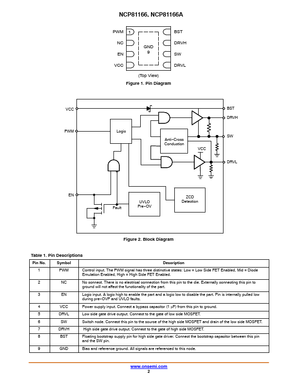
The PWM signal has three distinctive states: Low = Low Side FET Enabled, Mid = Diode Emulation Enabled, High = High Side FET Enabled. There is no electrical connection from this pin to the die.
NCP81166A Key Features
- Space-Efficient 2 mm x 2mm DFN8 Thermally-Enhanced Package
- VCC Range of 4.5 V to 13.2 V
- Integrated Bootstrap Diode
- Pre-OVP Function Protects Load during HS FET Short
- NCP81166: 2.25 V SW Trip Threshold
- NCP81166A: 1.8 V SW Trip Threshold
- Zero Current Detect Function Provides Power Saving Operation
- Bi-directional Enable Feature pulls Enable pin low during pre-OVP
- 5 V tri-state PWM Logic
- Adaptive Anti-Cross-Conduction Circuit Protects against
NCP81166A Applications
- Power Solutions for Desktop Systems