NCV57302 Description
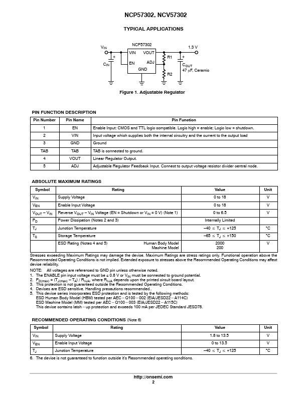
Pin Number Pin Name Pin Function 1 EN Enable Input: CMOS and TTL logic patible. 2 VIN Input voltage which supplies both the internal circuitry and the current to the output load 3 GND Ground TAB TAB TAB is connected to ground.
NCV57302 Key Features
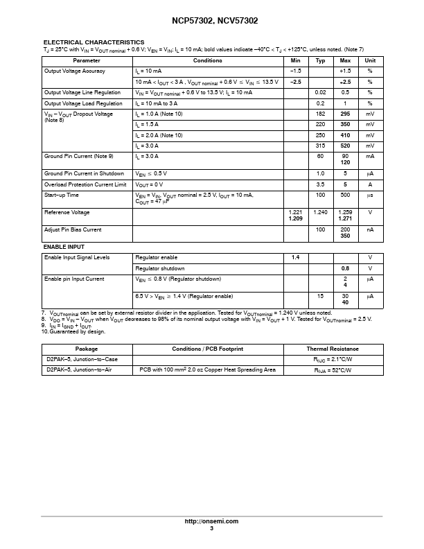
- Output Current in Excess of 3.0 A
- Minimum Operating Input Voltage 1.8 V for Full 3 A Output Current
- 315 mV Typical Dropout Voltage at 3.0 A
- Adjustable Output Voltage Range from 1.24 V to 13 V
- Low Ground Current
- Fast Transient Response
- Stable with Ceramic Output Capacitor
- Logic patible Enable Pin
- Current Limit, Reverse Current and Thermal Shutdown Protection
- Operation up to 13.5 V Input Voltage