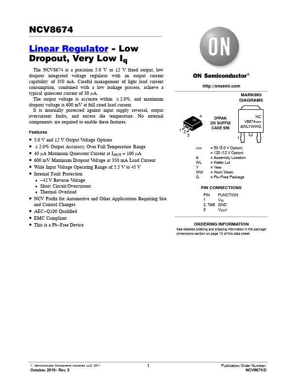
NCV8674 Description
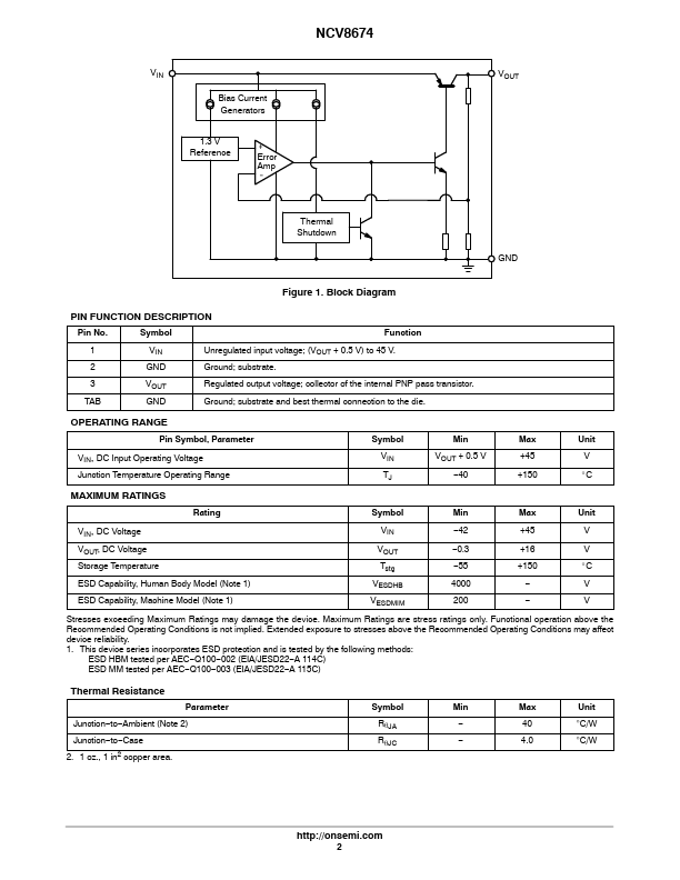
Symbol Function 1 VIN Unregulated input voltage; 3 VOUT Regulated output voltage; collector of the internal PNP pass transistor.
NCV8674 Key Features
- 5.0 V and 12 V Output Voltage Options
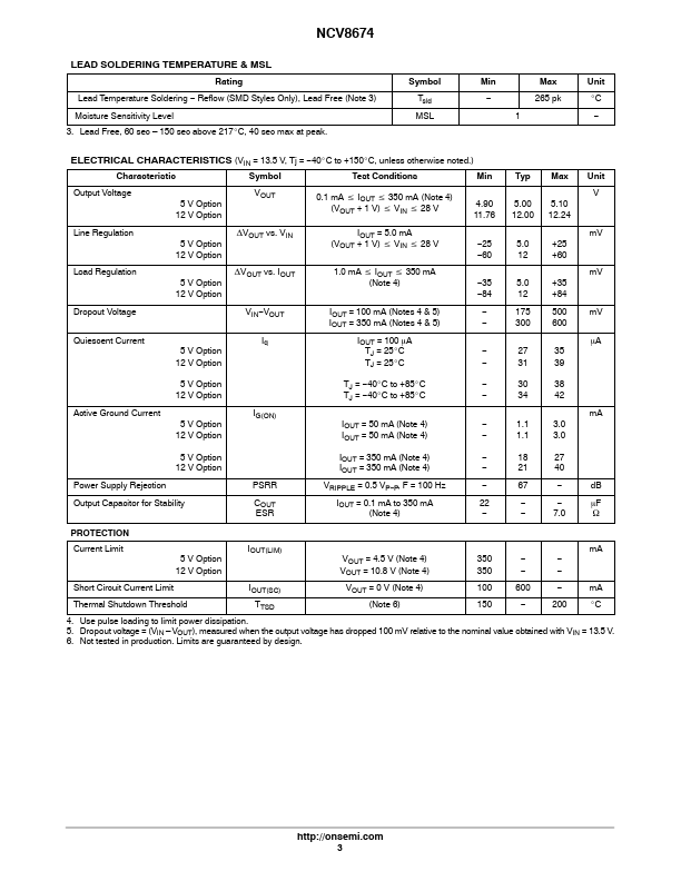
- "2.0% Output Accuracy, Over Full Temperature Range
- 40 mA Maximum Quiescent Current at IOUT = 100 mA
- 600 mV Maximum Dropout Voltage at 350 mA Load Current
- Wide Input Voltage Operating Range of 5.5 V to 45 V
- Internal Fault Protection
- 42 V Reverse Voltage
- Short Circuit/Overcurrent
- Thermal Overload
- NCV Prefix for Automotive and Other