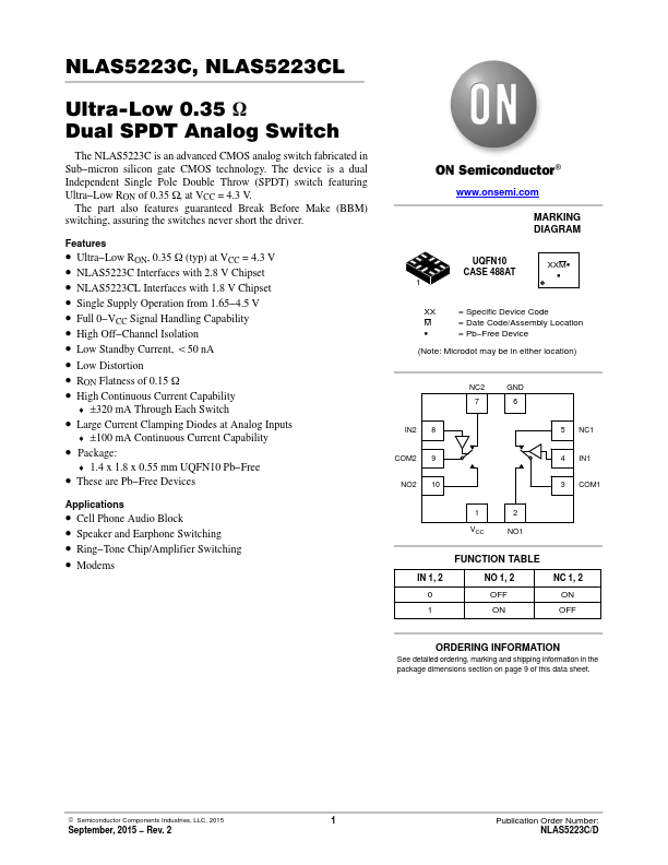
NLAS5223C Description
If any of these limits are exceeded, device functionality should not be assumed, damage may occur and reliability may be affected. Defined as 10% ON, 90% OFF Duty Cycle. REMENDED OPERATING CONDITIONS Symbol Parameter Min Max Unit VCC DC Supply Voltage 1.65 4.5 V VIN Digital Select Input Voltage (OVT) Overvoltage Tolerance GND 4.5 V VIS Analo.
NLAS5223C Key Features
- Ultra-Low RON, 0.35 W (typ) at VCC = 4.3 V
- NLAS5223C Interfaces with 2.8 V Chipset
- NLAS5223CL Interfaces with 1.8 V Chipset
- Single Supply Operation from 1.65-4.5 V
- Full 0-VCC Signal Handling Capability
- High Off-Channel Isolation
- Low Standby Current, t50 nA
- Low Distortion
- RON Flatness of 0.15 W
- High Continuous Current Capability