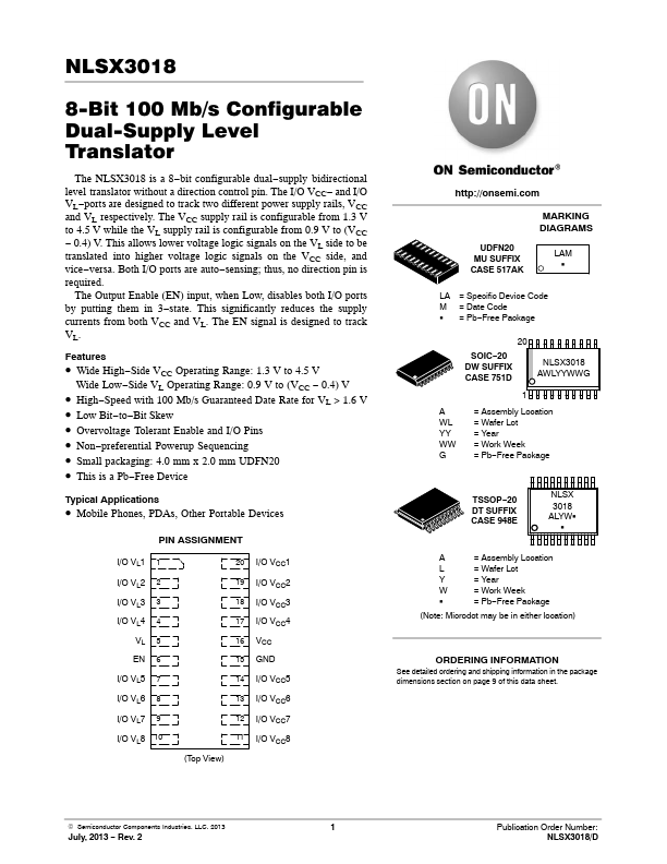
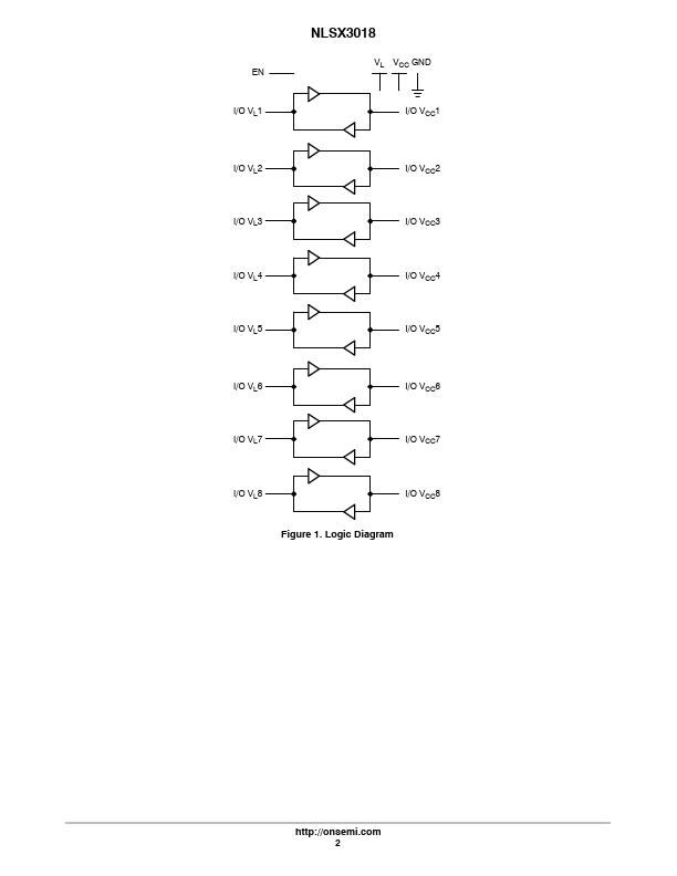
NLSX3018 Description
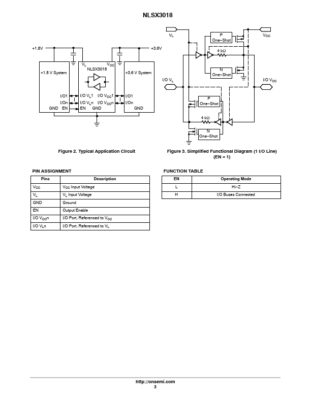
VCC VL GND VCC Input Voltage VL Input Voltage Ground EN Output Enable I/O VCCn I/O VLn I/O Port, Referenced to VCC I/O Port, Referenced to VL Figure 3. Simplified Functional Diagram (1 I/O Line) (EN = 1) FUNCTION TABLE EN L H Operating Mode Hi−Z I/O Buses Connected http://onsemi.
NLSX3018 Key Features
- Wide High-Side VCC Operating Range: 1.3 V to 4.5 V
- 0.4) V
- High-Speed with 100 Mb/s Guaranteed Date Rate for VL > 1.6 V
- Low Bit-to-Bit Skew
- Overvoltage Tolerant Enable and I/O Pins
- Non-preferential Powerup Sequencing
- Small packaging: 4.0 mm x 2.0 mm UDFN20
- This is a Pb-Free Device