PCS3P622Z05C Description
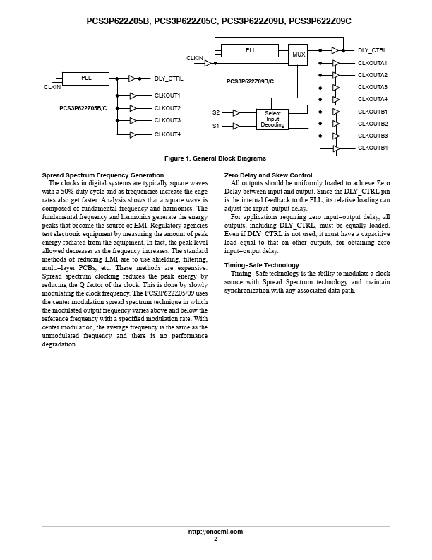
PCS3P622Z05/09 is a versatile, 3.3 V Zero−delay buffer designed to distribute low frequency Timing−Safe clocks with Peak EMI reduction. PCS3P622Z05 is an eight−pin version, accepts one reference input and drives out five low−skew Timing−Safe clocks. PCS3P622Z09 accepts one reference input and drives out nine low−skew Timing−Safe clocks.
PCS3P622Z05C Key Features
- Low Frequency Clock Distribution with Timing-Safe Peak EMI
- Input Frequency Range: 4 MHz
- 20 MHz
- Multiple Low Skew Timing-Safe Outputs
- External Input-Output Delay Control Option
- Supply Voltage: 3.3 V ± 0.3 V
- mercial and Industrial Temperature Range
- Packaging Information
- True Drop-in Solution for Zero Delay Buffer, ASM5P2305A / 09A
- These Devices are Pb-Free, Halogen Free/BFR Free and are RoHS