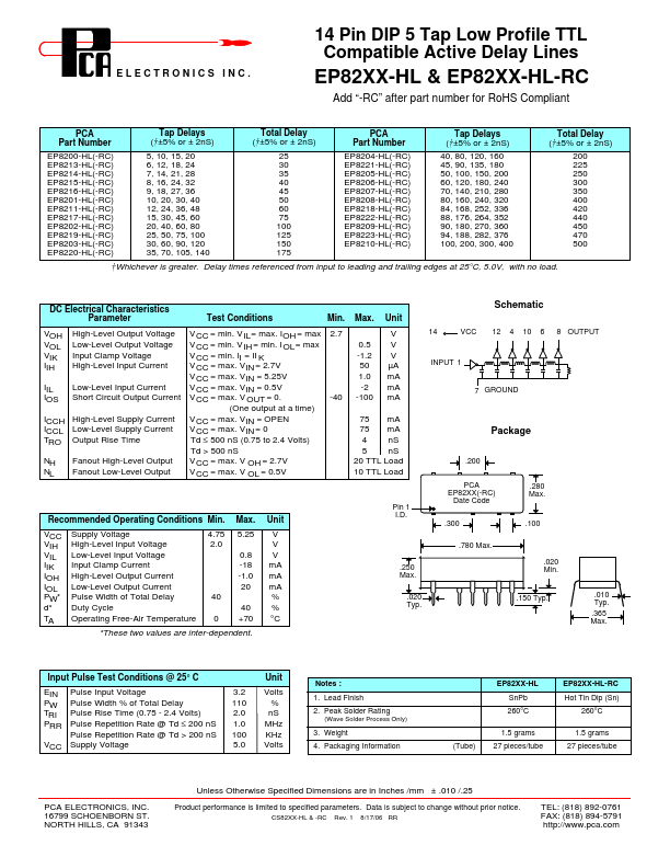
Parameter Test Conditions Min. Max. Unit Schematic VOH High-Level Output Voltage VCC = min. VIL= max. IOH = max 2.7 VOL Low-Level Output Voltage VCC = min. VIH = min. IOL= max VIK Input Clamp Voltage VCC = min. II = II K IIH High-Level Input Current VCC = max. VIN = 2.7V VCC = max. VIN = 5.25V IIL Low-Level Input Current VCC = max. VIN = 0.5V IOS Short Circuit Output Current VCC = max. V OUT = 0. -40 (One output at a time) ICCH High-Level Supply Current ICCL Low-Level Supply Current TRO Output Rise Time VCC = max. VIN = OPEN VCC = max. VIN = 0 Td ≤ 500 nS (0.75 to 2.4 Volts) Td > 500 nS NH Fanout High-Level Output VCC = max. V OH = 2.7V NL Fanout Low-Level Output VCC = max. V OL = 0.5V Recommended Operating Conditions Min. Max. Unit VCC VIH VIL IIK IOH IOL PW* d* Supply Voltage High-Level Input Voltage Low-Level Input Voltage Input Clamp Current High-Level Output Current Low-Level Output Current Pulse Width of Total Delay Duty Cycle 4.75 5.25 V 2.0 V 0.8 V -18 mA -1.0 mA 20 mA 40 % 40 % TA Operating Free-Air Temperature 0 +70 °C *These two values are inter-dependent.
This website uses cookies or similar technologies, to enhance your browsing experience and provide personalized recommendations. By continuing to use our website, you agree to our Privacy Policy