Datasheet Summary
PG 12856-A
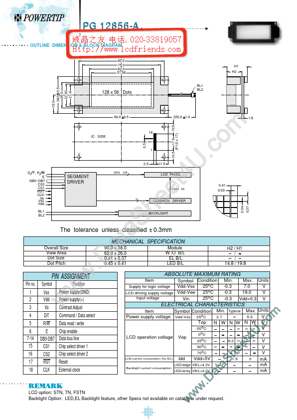
OUTLINE DIMENSION & BLOCK DIAGRAM
45.0 82.0 75.0 62.0 57.56 H1 H2
19.0 38.0 0.5 26.0 22.92 21.0
128 x 56 Dots
BL1 BL2
90.0 0.5
250.0 1.0 10.5 17.0 (P1.0 x 17)
18 IC SIDE 0.5
2.5 D I,R W E DB0~DB7 CS2 CS1 RST CLK Vo Vss Vdd BL1 BL2
SEG 128
11.5 LCD PANEL
SEGMENT DRIVER
The tolerance unless classified
Overall Size View Area Dot Size Dot Pitch
MECHANICAL SPECIFICATION
PIN ASSIGNMENT
Pin no. Symbol Function
1 2 3 4 5 6 7-14 15 16 17 18
Vss Vdd Vo D/I R/W E DB0-DB7 CS1 CS2 RST CLK
Power supply(GND) Power supply(+) Contrast Adjust mand / Data select Data read / write Chip enable Data bus line Chip select driver 1 Chip select driver 2 Reset External clock...