Datasheet4U.com
🌙
pg240160ca1
PG240160-B
PG240160_B
PG240160_C_A1
pg240160b
pg240160ca1 Datasheet | POWERTIP
Part:
pg240160ca1
Description:
LCD_Module
Manufacturer:
POWERTIP
Size:
163.27 KB
pg240160ca1 Datasheet (PDF) Download
POWERTIP
pg240160ca1
Key Features
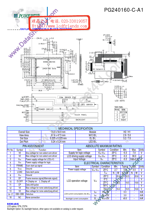
20.2 18.2 16.2
DD DD DD IEE EL OP
20.8 18.8 16.8
×
Close