PT7V2727
PT7V2727 is VCXO 3.3v/5.0v operating voltage manufactured by PT.
Description
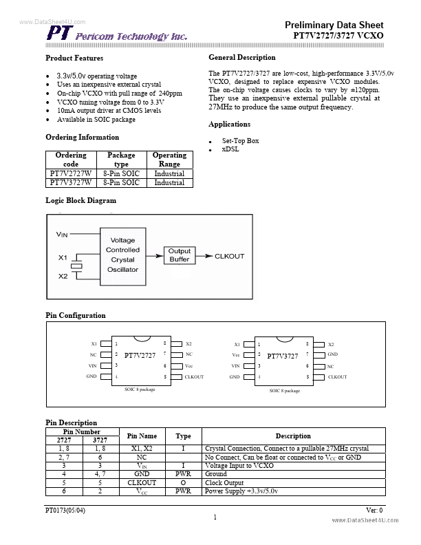
The PT7V2727/3727 are low-cost, high-performance 3.3V/5.0v VCXO, designed to replace expensive VCXO modules. The on-chip voltage causes clocks to vary by ±120ppm.
|||||||||||||||||||||||||||||||||||||||||||||||||||||||||||||||||||||||||||||||||||||||||||||||||||||||||||||||||||||||||||||||||||||||||||||||||||||||||||||||||||||||||||||||||||||||||||||||||||||||||||||||||||||||||||||||||||||||||||||||||||||||||||||||||||||||||||||||||||||||||||||||||||||||||||||||||||||||||||||||||||||||
Product Features
- -
- -
- - 3.3v/5.0v operating voltage Uses an inexpensive external crystal On-chip VCXO with pull range of 240ppm VCXO tuning voltage from 0 to 3.3V 10m A output driver at CMOS levels Available in SOIC package
They use an inexpensive external pullable crystal at 27MHz to produce the same output frequency. Applications z z
Ordering Information Ordering code PT7V2727W PT7V3727W Package type 8-Pin SOIC 8-Pin SOIC Operating Range Industrial Industrial
Set-Top Box x DSL
Logic Block Diagram
Pin Configuration
X1 NC VIN GND
1 2 3 4 SOIC 8 package
X2 NC Vcc CLKOUT
X1 Vcc VIN GND
1 2 3 4 SOIC 8 package
X2 GND NC CLKOUT
7 6 5
PT7V3727
7 6 5
Pin Description
Pin Number 2727 3727 1, 8 1, 8 2, 7 6 3 3 4 4, 7 5 5 6 2
PT0173(05/04) 1
Pin Name X1, X2 NC VIN GND CLKOUT VCC
Type I I PWR O PWR
Description
Crystal Connection, Connect to a pullable 27MHz crystal No Connect, Can be float or connected to VCC or GND Voltage Input to VCXO Ground Clock Output Power Supply +3.3v/5.0v
Ver: 0
..
Preliminary Data Sheet PT7V2727/3727 VCXO
|||||||||||||||||||||||||||||||||||||||||||||||||||||||||||||||||||||||||||||||||||||||||||||||||||||||||||||||||||||||||||||||||||||||||||||||||||||||||||||||||||||||||||||||||||||||||||||||||||||||||||||||||||||||||||||||||||||||||||||||||||||||||||||||||||||||||||||||||||||||||||||||||||||||||||||||||||||||||||||||||||||||
Maximum Ratings
(Above which the useful life may be impaired. For user guidelines, not...