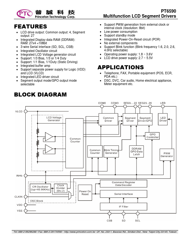
PT6590 Overview
Description
Chip select: "L" active Serial data transfer clock Input serial data Power supply for LOGIC Display turning on/off select terminal H: turning on display, L: turning off display INHb=“L”: All SEG/COM terminal: output VSS level GPO terminal: output VSS level LED drive terminal: output Hi-Z External clock input terminal (for display/PWM using selectable) Must be connect t.
Key Features
- LCD drive output: Common output: 4, Segment output: 27
- Integrated Display data RAM (DDRAM): RAM: 27x4 =108bit
- 3-wire Serial interface (SD, SCL, CSB)
- Integrated Oscillator circuit
- Integrated LCD Voltage generator circuit