P75N75
P75N75 is 75V N-Channel MOSFET manufactured by PanJit Semiconductor.
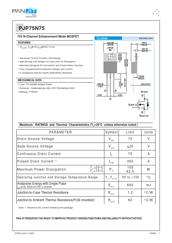
PJP75N75
75V N-Channel Enhancement Mode MOSFET
Features
- RDS(ON), VGS@10V,IDS@30A=11mΩ
- Advanced Trench Process Technology
- High Density Cell Design For Ultra Low On-Resistance
- Specially Designed for Converters and Power Motor Controls
- Fully Characterized Avalanche Voltage and Current
- In pliance with EU Ro HS 2002/95/EC directives
MECHANICAL DATA
- Case: TO-220AB Molded Plastic
- Terminals : Solderable per MIL-STD-750,Method 2026
- Marking : P75N75
Drain
Gate
Source
Maximum RATINGS and Thermal Characteristics (TA=25OC unless otherwise noted )
PARAMETER
Symbol Limit
Drain-Source Voltage
VDS 75
Gate-Source Voltage
VGS +20
Continuous Drain Current
ID 7 5
Pulsed Drain Current 1)
ID M
Maximum Power Dissipation
TA =25OC TA =75OC
Op e ra ti ng J unc ti o n a nd S to ra g e Te mp e ra ture Ra ng...