PJDLLLC05
PJDLLLC05 is Low Capacitance TVS Diode Array manufactured by PanJit Semiconductor.
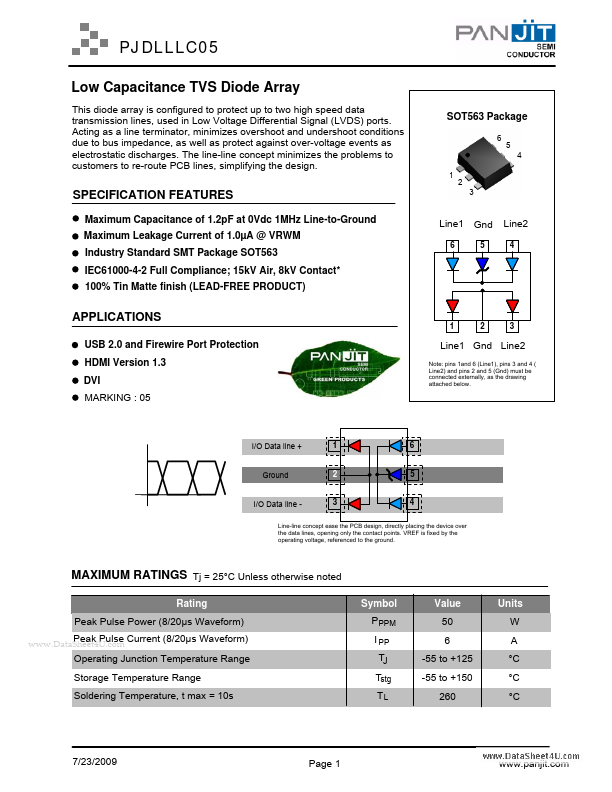
FEATURES
Maximum Capacitance of 1.2p F at 0Vdc 1MHz Line-to-Ground Maximum Leakage Current of 1.0µA @ VRWM Industry Standard SMT Package SOT563 IEC61000-4-2 Full pliance; 15k V Air, 8k V Contact- 100% Tin Matte finish (LEAD-FREE PRODUCT)
Line1
Gnd
Line2
APPLICATIONS
USB 2.0 and Firewire Port Protection HDMI Version 1.3 DVI
Line1 Gnd Line2
Note: pins 1and 6 (Line1), pins 3 and 4 ( Line2) and pins 2 and 5 (Gnd) must be connected externally, as the drawing attached below.
MARKING : 05
I/O Data line + Ground I/O Data line
- 1
Line-line concept ease the PCB design, directly placing the device over the data lines, opening only the contact points. VREF is fixed by the operating voltage, referenced to the ground.
MAXIMUM RATINGS Tj = 25°C Unless otherwise noted
Rating Peak Pulse Power (8/20µs Waveform)
..
Symbol P PPM I PP TJ Tstg TL
Value 50 6 -55 to +125 -55 to +150 260
Units W A °C °C °C
Peak Pulse Current (8/20µs Waveform) Operating Junction Temperature Range Storage Temperature Range Soldering Temperature, t max = 10s
7/23/2009
Page 1
.panjit.
ELECTRICAL CHARACTERISTICS
Parameter Reverse Stand-Off Voltage Reverse Breakdown Voltage Reverse Leakage Current Clamping Voltage (8/20µs) Clamping Voltage (8/20µs) Clamping Voltage (8/20µs) Off State Junction Capacitance Symbol VWRM VBR IR Vc Vc Vc Cj I BR = 1m A VR = 5V I pp = 1 A I pp = 2 A I pp = 5 A
0 Vdc Bias f = 1MHz Between I/O pins and GND 0 Vdc Bias f = 1MHz Between I/O pins
Tj = 25°C unless otherwise noted
Conditions Min Typical Max 5 6.2 1.0 10 12 15 1.0 1.0 Units V V µA V V V p F p...