PJESDZ6V8-2G
PJESDZ6V8-2G is E.S.D. Dual Protection Diode Array manufactured by PanJit Semiconductor.
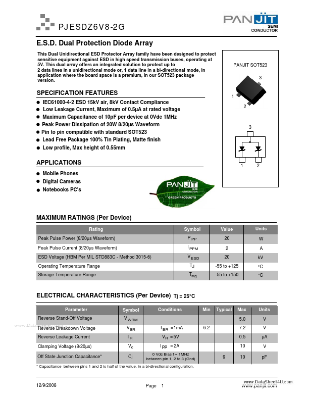
FEATURES
IEC61000-4-2 ESD 15k V air, 8k V Contact pliance Low Leakage Current, Maximum of 0.5µA at rated voltage Maximum Capacitance of 10p F per device at 0Vdc 1MHz Peak Power Dissipation of 20W 8/20µs Waveform Pin to pin patible with standard SOT523 Lead Free Package 100% Tin Plating, Matte finish Low profile, Max height of 0.55mm
1 2
APPLICATIONS
Mobile Phones Digital Cameras Notebooks PC's
MAXIMUM RATINGS (Per Device)
Rating Peak Pulse Power (8/20µs Waveform) Peak Pulse Current (8/20µs Waveform) ESD Voltage (HBM Per MIL STD883C
- Method 3015-6) Operating Temperature Range Storage Temperature Range Symbol P PP I PPM V ESD TJ Tstg Value 20 2 20 -55 to +125 -55 to +150 Units W A k V °C °C
ELECTRICAL CHARACTERISTICS (Per Device) Tj = 25°C
Parameter Reverse Stand-Off Voltage Symbol V WRM VBR IR Vc Cj I BR = 1m A VR = 5V I pp = 2A
0 Vdc Bias f = 1MHz between pin 1, 2 to 3 (Gnd)
Conditions
Min
Typical
Max 5.0
Units V V µA V p F
.. Reverse Breakdown Voltage
Reverse Leakage Current Clamping Voltage (8/20µs) Off State Junction Capacitance-
7.2 0.5 10 9 10
- Capacitance between pins 1 and 2 is half of the value, in a bi-directional configuration.
12/9/2008
Page
.panjit.
TYPICAL CHARACTERISTIC CURVES (Per Device)
Tj = 25°C
Pulse Waveform 110 100 90 80 Percent of Ipp 70 60 50 40 30 20 10 0 0 5 10 15 time, µsec 20 25 30 Rise time 10-90%
- 8µs 50% of Ipp @ 20µs
Clamping Voltage vs 8/20µs Ipp
9.5 9 Clamping Voltage, V 8.5 8 7.5 7 6.5 0 0.5 1 1.5 Peak Current, A 8/20µs 2
Off-State Capacitance vs DC Bias
10 Junction Capacitnace, p F 9 8 7 6 5 4 0 1 2 3 Vdc Bias, V 4 5
..
12/9/2008
Page...