PJSD05CFN2
PJSD05CFN2 is BI-DIRECTIONAL TVS manufactured by PanJit Semiconductor.
BI-DIRECTIONAL TVS
This bi-directional TVS has been designed to protect sensitive equipment against ESD and to prevent Latch-Up events in CMOS circuitry operating at 5Vdc and below.This offers an integrated solution to protect a single data line where the board space is a premium.
SPECIFICATION FEA TURES
- 200W Power Dissipation (8/20s Waveform)
- Low Leakage Current, Maximum of 1 A@5Vdc
- Very low Clamping voltage
- IEC 61000-4-2 ESD 15k V air, 8k V Contact pliance
- In pliance with EU Ro HS 2002/95/EC directives
- Terminals : Solderable per MIL-STD-750, Method 2026
- Case : DFN 2L, Plastic
- Marking : BT
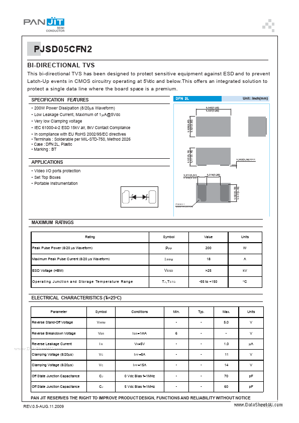
2 7 5 4
DFN 2L
Unit : inch(mm)
APPLICATIONS
- Video I/O ports protection
- Set Top Boxes
- Portable Instrumentation
2 47 5 4
3 2 0.008(0.22)
MAX.
PIN NO.1 IDENTIFICATION
MAXIMUM RA TINGS
Rating Peak Pulse Power (8/20 s Waveform) Maximum Peak Pulse Current (8/20 s Waveform) ESD Voltage (HBM) Op e ra ti ng J unc ti o n a nd S to r a g e Te m p e r a ture R a ng e Symbol Value 200 18 >25 -55 to +150 Units W A k V
PPP I PPM VESD
T J ,T S TG
ELECTRICAL CHARACTERISTICS (T A=25o C)
Parameter Reverse Stand-Off Voltage Reverse Breakdown Voltage Reverse Leakage Current Symbol VWRM VBR IR VC VC CJ CJ I BR =1m A VR=5V I PP =5A I PP =15A 0 Vdc Bias f=1MHz 5 Vdc Bias f=1MHz Conditions Min. 6 Typ. Max. 5.0 1.0 11 14 70 60 Units V V A V V p F p F
..
Clamping Voltage (8/20s) Clamping Voltage (8/20s) Off State Junction Capacitance Off State Junction Capacitance
PAN JIT RESERVES THE RIGHT TO IMPROVE PRODUCT DESIGN, FUNCTIONS AND RELIABILITY WITHOUT NOTICE REV.0.5-AUG.11.2009 PAGE . 1
TYPICAL CHARACTERISTICS
100 90
Per cen t of I pp
80 70 60 50 40 30 20 10
50% of I pp@20 m s...