2SB1548A
Key Features
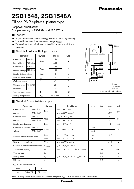
- 0±0.5 s Absolute Maximum Ratings Parameter Collector to base voltage Collector to 2SB1548 2SB1548A 2SB1548 Symbol VCBO VCEO VEBO ICP IC PC Tj Tstg (TC=25˚C) Ratings -60 -80 -60 -80 -5 -5 -3 25 2 150 -55 to +150 Unit V φ3.2±0.1
- 7±0.2 4.2±0.2
- 4±0.2 1.6±0.2 0.8±0.1 2.54±0.3 3 5.08±0.5
- 0±0.5 High forward current transfer ratio hFE which has satisfactory linearity Low collector to emitter saturation voltage VCE(sat) Full-pack package which can be installed to the heat sink with one screw
- 9±0.3
- 6±0.2 2.9±0.2
- 6±0.1 emitter voltage 2SB1548A Emitter to base voltage Peak collector current Collector current Collector power TC=25°C dissipation Ta=25°C Junction temperature Storage temperature V V
- 55±0.15 1 2 A A W ˚C ˚C 1:Base 2:Collector 3:Emitter TO-220D Full Pack Package s Electrical Characteristics Parameter Collector cutoff current Collector cutoff current Emitter cutoff current Collector to emitter voltage 2SB1548 2SB1548A 2SB1548 2SB1548A 2SB1548 2SB1548A (TC=25˚C) Symbol ICES ICEO IEBO VCEO hFE1* hFE2 VBE VCE(sat) fT ton tstg tf IC = -1A, IB1 = - 0.1A, IB2 = 0.1A Conditions VCE = -60V, VBE = 0 VCE = -80V, VBE = 0 VCE = -30V, IB = 0 VCE = -60V, IB = 0 VEB = -5V, IC = 0 IC = -30mA, IB = 0 VCE = -4V, IC = -1A VCE = -4V, IC = -3A VCE = -4V, IC = -3A IC = -3A, IB = - 0.375A VCE = -10V, IC = - 0.5A, f = 10MHz 30 0.5 1.2 0.3 -60 -80 70 10 -1.8 -1.2 V V MHz µs µs µs 250 V min typ max -200 -200 -300 -300 -1 Unit µA µA mA Forward current transfer ratio Base to emitter voltage Collector to emitter saturation voltage Transition frequency Turn-on time Storage time Fall time
- h FE1 Rank classification Q 70 to 150 P 120 to 250 Rank hFE1 Note: Ordering can be made by the common rank (PQ rank hFE1 = 70 to 250) in the rank classification. 1 Power Transistors PC - Ta