AN3371SB
Key Features
- 25 - 0.05 + 0.1 tion frequency with external constants.
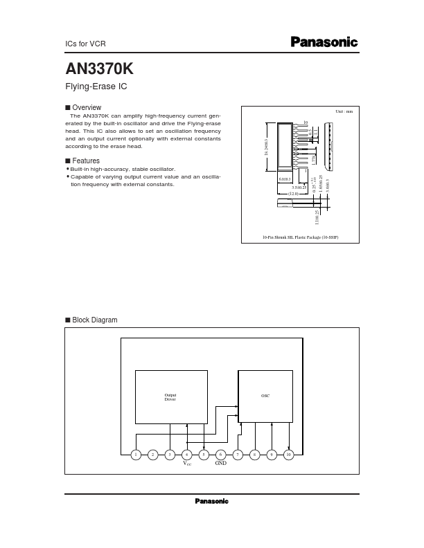
- 5±0.25 (12.0) 10-Pin Shrunk SIL Plastic Package (10-SSIP) s Block Diagram Output Driver OSC 1 2 3 4 5 6 7 8 9 10 VCC GND
- 1±0.25
- 0±0.3
- 65±0.25
- Built-in high-accuracy, stable oscillator.
- Capable of varying output current value and an oscilla- 1
- 778 AN3370K s Absolute Maximum Ratings (Ta=25˚C) Parameter Supply voltage Power dissipation Operating ambient temperature Storage temperature Symbol VCC PD Topr Tstg Rating 12.6 500 - 20 to + 70 - 55 to +150 ICs for VCR Unit V mW ˚C ˚C s Remended Operating Range (Ta = 25˚C) Parameter Operating supply voltage range Symbol VCC Range 10.5V to 12.5V s Electrical Characteristics (VCC=12V, Ta=25˚C) Parameter Supply current Oscillation output amplitude Oscillation frequency Oscillation output amplitude Flying ON Flying OFF Symbol ICC VO1 fO VO2 V1H V1L V1= 5V V1= 5V, RL= 300Ω V1= 5V, RL= 300Ω V1= 0V, RL= 300Ω 3.5 0.8 Condition min 20 8 11 typ 28 9 11.55 12.1 10 max 36 Unit mA VPP MHz mVPP V V s Application Circuit Output Driver OSC 1 2 3 0.01 µF 0.01µF 4 1.8kΩ 5 6 7 8 9 10 56pF 5.1kΩ 33pF 0.01µF 68pF 68pF 100µF
- 7µH 4µH Flying Control Voltage VCC=12V Note) Do not apply a voltage (0V included) to the Pin2 from the external. ICs for VCR s Pin Descriptions Pin No. Pin name Typ. waveform Description I/O impedance AN3370K Equivalent circuit 1 1 Flying erase control pin Flying erase ON/OFF control pin. ON when 3.5V or more is applied, and OFF when 0.8V or less is applied. 3MΩ 30kΩ 30kΩ 2 30kΩ 30kΩ 2 Do not apply a voltage from the external. 60kΩ 5 3 Feedback pin Feedback pin to obtain a DC voltage by filtering an output signal via an external capacitor 10kΩ 3 4 Power supply Power supply pin. Apply 12V typically from the external. 5 Output pin 6V High-frequency current 10kΩ 5 10kΩ 3 6 GND 7 Oscillation input pin It is possible to change the current which can be taken out of an output, by varying the resistor between this pin and GND. NPN Tr emitter 2V 7 8 Reference voltage pin Generates a reference voltage of 1/2 VCC (approx. 6V) NPN Tr emitter 6V 8 9 Oscillation feedback pin
- 4V A signal from Pin10 oscillation output is divided by the capacitor and is fed back. 3kΩ 3kΩ 9 10 Oscillation output pin 6V Oscillates at the frequency determined by L, C of the Pins8, 9, 10