AN6783S
Key Features
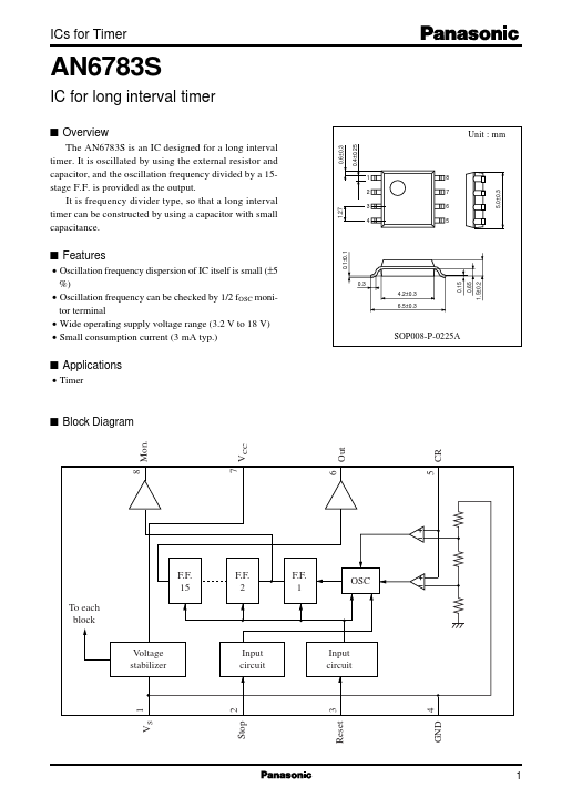
- Timer s Block Diagram Mon. VCC Out CR OSC 8 7 6 F.F. 15 To each block Voltage stabilizer F.F. 2 F.F. 1 Input circuit Input circuit 1 2 3 Stop Reset VS GND 4 5 1 AN6783S s Pin Descriptions Pin No. 1 2 3 4 5 6 7 8 Symbol VS Stop Reset GND CR Out VCC Mon. Description Reference voltage Oscillation stop input Reset input Grounding C and R connection Output Supply voltage Monitor pin ICs for Timer s Absolute Maximum Ratings Parameter Supply voltage Supply current Power dissipation Operating ambient temperature Storage temperature
- Symbol VCC ICC PD Topr Tstg VSTOP VRESET VCR IOUT Rating 20 7 140 -35 to +85 -55 to +125 0 to 18 0 to 18 0 to 3 -15 to +15 Unit V mA mW °C °C V V V mA Stop terminal voltage Reset terminal voltage CR terminal voltage Out terminal current Note)
- Do not apply external currents or voltages to any pins not specifically mentioned. For circuit currents, '+' denotes current flowing into the IC, and '-' denotes current flowing out of the IC. 2. *: Except for the operating ambient temperature and storage temperature, all ratings are for Ta = 25°C. s Recommended Operating Range Parameter Supply voltage Symbol VCC Range 3.2 to 18.0 Unit V s Electrical Characteristics at Ta = 25°C Parameter Quiescent supply current Internal reference voltage High-level input current Low-level input current High-level out terminal voltage Low-level out terminal voltage Symbol ICC VS IIH IIL VOH VOL Conditions VCC = 5 V VCC = 5 V, IS = -3 mA VCC = 18 V, VIH = 18 V VCC = 18 V, VIL = 0 V VCC = 18 V, IOH = -10 mA VCC = 3.2 V, IOL = -10 mA Min 2.0 2.40 -100 14.0 Typ 4.0 2.55 16.0 Max 5.0 2.70 10 18.0 0.4 Unit mA V µA µA V V 2 ICs for Timer s Electrical Characteristics at Ta = 25°C (continued) Parameter High-level Mon. terminal voltage Low-level Mon. terminal voltage Oscillation frequency precision Oscillation frequency fluctuation with supply voltage High-level input voltage Low-level input voltage
- Design reference data Symbol VMH VML fOSC ∆ fV VIH VIL Conditions VCC = 18 V VCC = 3.2 V VCC = 5 V, RT = 1 kΩ, CT = 0.1 µF VCC = 5 V, 3.2 V to 18.0 V VCC = 5 V VCC = 5 V -5.0 2.0 Min 17.8 9.0 Typ 9.5 AN6783S Max 18.0 0.4 10.0 5.0 0.8 Unit V V kHz % V V Note) The characteristic values below are theoretical values for designing and not guaranteed. The data show the changing amount within Ta = -35°C to +85°C when the values at Ta = 25°C is taken as the reference. Parameter Oscillation frequencytemperature dependency Symbol ∆ fr Conditions VCC = 5 V, RT = 1 kΩ, CT = 0.1 µF Min -5.0 Typ Max 5.0 Unit % s Terminal Equivalent Circuits Pin No. 1 Equivalent circuit Description VS : Stabilized power supply output terminal. Reference voltage source for oscillation circuit. Stop : Oscillation stop input terminal. Only the oscillation circuit stops when this terminal becomes low-level. (F.F. is not cleared) When not used, the terminal should be open or connected to VCC . I/O O DC voltage 2.55 V 2 VS VCC I Stop 3 AN6783S s Terminal Equivalent Circuits (continued) Pin No. 3 Equivalent circuit VS VCC Description Reset : Reset input terminal. F.F. is reset when the terminal becomes low-level and is set in the initial state. When not used, the terminal should be open or connected to VCC . The reset is applied by rising VCC from a voltage below 0.8 V (power-on reset function). GND : Grounding terminal. CR : C and R connection terminal. The oscillation period is determined by an external resistor and capacitor. When applying a pulse to this terminal from the outside, the voltage should be within the range of 0 V to 3 V. ICs for Timer I/O I DC voltage Reset 4 5 0V 0.7 V to 1.8 V CR VS 6 VCC Out Out : Output terminal. A frequency which is 1/32768 of the oscillation frequency is outputted. Use with an output current within ±10 mA. O High-level VCC -1.4 V Low-lebel < 0.4 V 7 8 VCC VCC : Supply voltage terminal. Mon. : Oscillation frequency monitor terminal. The output is given from the first stage of F.F. and a frequency which is 1/2 of the oscillation frequency fOSC is outputted. If not used, the terminal should be open. This terminal is provided for connecting probe such as oscilloscope. Use it with an output current under 100 µA. O High-level VCC Low-level < 0.4 V RA = 10 kΩ to 40 kΩ Mon. 4 ICs for Timer s Usage Notes AN6783S Pay attention to the following matters in order to prevent the destruction during the use and to increase the reliability ;
- In the application circuit example, the calculated value by the theoretical equation for timer interval calculation and the characteristics curve vary depending on the precision of the time interval capacitor used in the actual set. Take such matter of the above into consideration. Also, the proportional constant α depends on the kinds and characteristics of the time interval resistor and time interval capacitor. Make a final confirmation with the finished products. In the case when a high precision is required, adjust the value by using a variable resistor as the time interval resistor.
- Use a time interval resistor in the range of 1 kΩ to 1 MΩ, and a time interval capacitor in the range of 0.1 µF to 100 µF which is polyester or tantalum electrolytic capacitor with a small tanδ value.
- Connect a capacitor (1 µF to 10 µF) to the VS terminal in order to protect the IC from an external noise and stabilize its operation.
- If turning on power again after an extremely short-time power supply off state during the normal operation, be careful that there may be a case that the automatic reset (power-on reset) fails due to a residual potential of the external capacitance.
- Take measures against noise in order to avoid the malfunction caused by the external noise. Pay attention to the noise from an external source especially at setting a long interval time.
- When connecting a plunger or relay to the output circuit, connect a diode to the both ends of coil in order to protect the IC from the counter-electromotive force generted after the circuit is turned off .