AN7118S
Overview
- Low voltage operation : VCC = 1.8V to 4.5V
- Reduced voltage operation is available.
- Low pop noise when supply voltage is switched
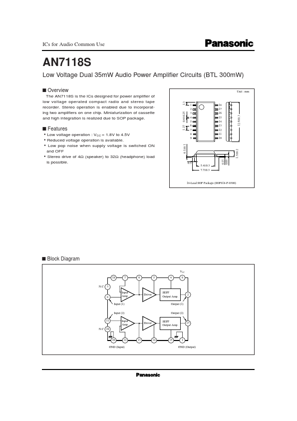
- 4±0.3 7.7±0.3 18-Lead SOP Package (SOP018-P-0300) s Block Diagram VCC 18 N.C 3 Input Amp. Input (1) Input (2) 11 N.C 16 Input Amp. Driver Driver SEPP Output Amp. Output (1) Output (2) SEPP Output Amp. 17 2 7 6 5 4 9 8 10 12 13 14 15 1 GND (Output) GND (Input)
- 15 0.65 ON and OFF
- Stereo drive of 4Ω (speaker) to 32Ω (headphone) load is possible.
- 5±0.2
- 6±0.3 AN7118S s Pin Descriptions Pin No. 1 2 3 4 5 6 7 8 9 Pin Name GND (Output) Output Ch.1 NC Bootstrap Phase Compensation Phase Compensation N.F.B Input Ch.1 VCC Pin No. 10 11 12 13 14 15 16 17 18 Pin Name GND (Input) Input Ch.2 N.F.B Phase Compensation Phase Compensation Bootstrap NC Output Ch.2 Ripple Filter ICs for Audio Common Use s Absolute Maximum Ratings (Ta= 25˚C) Parameter Supply Voltage Supply Current Power Dissipation Operating Ambient Temperature Storage Temperature Symbol VCC ICC PD Topr Tstg Rating 4.5 1 400 - 20 ~ + 75 - 50 ~ + 125 Unit V A mW ˚C ˚C s Electrical Characteristics (VCC = 3V, Ta = 25˚C) Parameter Quiescent Circuit Current Symbol ICQ GV PO THD Vno Ri RR VCC= 3V± 200mV, f= 100Hz Vi= 0mV Vi= 1.5mV, RL= 32Ω THD = 10%, RL= 32Ω × 2ch. Vi= 1.5mV, RL= 32Ω × 2ch. Rg= 10kΩ, DIN Audio Filter 45 Condition min. typ. 13 47 33 0.3 0.5 20 35 1 1 max. 18 49 Unit mA dB mW % mW kΩ dB <DUAL (f=1kHz)> Voltage Gain Maximum Output Total