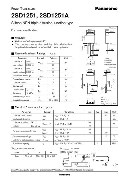
Datasheet4U Logo Datasheet4U.com

D1251 - 2SD1251

Key Features

  • q Wide area of safe operation (ASO) q N type package enabling direct soldering of the radiating fin to the printed circuit board, etc. of small electronic equipment. s Absolute Maximum Ratings (TC=25˚C) Parameter Symbol Ratings Collector to 2SD1251 base voltage 2SD1251A VCBO 60 80 Collector to 2SD1251 emitter voltage 2SD1251A VCEO 60 80 Emitter to base voltage Peak collector current Collector current Base current Collector power TC=25°C dissipation Ta=25°C VEBO ICP IC IB PC 8.

📥 Download Datasheet

Full PDF Text Transcription (Reference)

The following content is an automatically extracted verbatim text from the original manufacturer datasheet and is provided for reference purposes only.

View original datasheet text
Power Transistors 2SD1251, 2SD1251A Silicon NPN triple diffusion junction type For power amplification 8.5±0.2 6.0±0.5 Unit: mm 3.4±0.3 1.0±0.1 10.0±0.3 1.5±0.1 s Features q Wide area of safe operation (ASO) q N type package enabling direct soldering of the radiating fin to the printed circuit board, etc. of small electronic equipment. s Absolute Maximum Ratings (TC=25˚C) Parameter Symbol Ratings Collector to 2SD1251 base voltage 2SD1251A VCBO 60 80 Collector to 2SD1251 emitter voltage 2SD1251A VCEO 60 80 Emitter to base voltage Peak collector current Collector current Base current Collector power TC=25°C dissipation Ta=25°C VEBO ICP IC IB PC 8 6 4 1 30 1.