MN101C61
Overview
MN101C61D, MN101C61G Type ROM (× 8-bit) RAM (× 8-bit) Package Minimum Instruction Execution Time Standard: MN101C61D (under development) 64 K 3K TQFP080-P-1212D *Lead-free MN101C61G 128 K 12 K 0.1 µ...
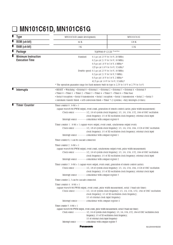
MN101C61D, MN101C61G Type ROM (× 8-bit) RAM (× 8-bit) Package Minimum Instruction Execution Time Standard: MN101C61D (under development) 64 K 3K TQFP080-P-1212D *Lead-free MN101C61G 128 K 12 K 0.1 µ...
| Part Number | Manufacturer | Description |
|---|---|---|
| MN101C61G | Matsushita Electric | MN101 Series microcontroller |
| MN101C61D | Matsushita Electric | MN101 Series microcontroller |
| MN101C62F | Matsushita Electric | MN101 Series microcontroller |
| MN101C67D | Matsushita Electric | MN101 Series microcontroller |
| MN101C67G | Matsushita Electric | MN101 Series microcontroller |