MN101D10G
MN101D10G is MN101D10x manufactured by Panasonic.
- Part of the MN101D10F comparator family.
- Part of the MN101D10F comparator family.
..
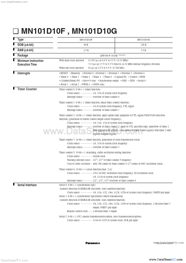
MN101D10F , MN101D10G
Type ROM (× 8-bit) RAM (× 8-bit) Package Minimum Instruction Execution Time Interrupts
With main clock operated When sub-clock operated MN101D10F 96 K 2.5 K QFP100-P-1818B
- Lead-free
MN101D10G 128 K 3.5 K
0.1397 µ s (at 4.0 V to 5.5 V, 14.32 MHz) 71.5 µ s (at 2.7 V to 5.5 V fixed to 14.32 MHz internal frequency division) 61 µ s (at 2.5 V to 5.5 V, 32.768 k Hz)
- RESET
- Runaway
- External 0
- External 1
- External 2
- External 3
- External 4
- Timer 0
- Timer 1
- Timer 2
- Timer 3
- Timer 6
- Capstan FG
- Control
- HSW
- Cylinder(Drum) FG
- Servo V-sync
- Synchronous output
- OSD
- XDS
- Serial 0
- Serial 1
- Serial 2
- PWM 4
- OSDV-sync Timer counter 0: 8-bit × 1 (timer function) Clock source
- -
- -
- -
- -
- -
- -
- -
-...