Datasheet4U.com
🌙
MN3307 Datasheet | Panasonic
Part:
MN3307
Description:
1024-Stage Ultra Low Voltage Operation BBD
Manufacturer:
Panasonic
Size:
86.09 KB
Download MN3307 Datasheet PDF
Related MN3307 Datasheets
MN3304 512-Stage Ultra Low Voltage Operation BBD for Audio Signals
Panasonic
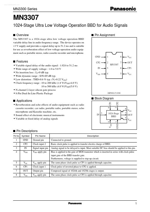
MN3307
Key Features
Variable signal delay of the audio signal : 1.024 to 51.2 ms
Wide range of supply voltage : 1.8 to 5.0 V
No insertion loss : Li=0 dB typ
Wide dynamic range : S/N=69 dB typ
Low distortion : THD=0.6 % typ. (Vi=0.22 Vrms)
×
Close