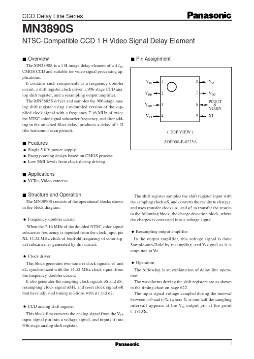
The following content is an automatically extracted verbatim text
from the original manufacturer datasheet and is provided for reference purposes only.
View original datasheet text
CCD Delay Line Series
MN3890S
NTSC-Compatible CCD 1 H Video Signal Delay Element
Overview
The MN3890S is a 1 H image delay element of a 4 fSC CMOS CCD and suitable for video signal processing applications. It contains such components as a frequency-doubler circuit, a shift register clock driver, a 906-stage CCD analog shift register, and a resampling output amplifier. The MN3885S drives and samples the 906-stage analog shift register using a redoubled version of the supplied clock signal with a frequency 7.16 MHz of twice the NTSC color signal subcarrier frequency, and after adding in the attached filter delay, produces a delay of 1 H (the horizontal scan period).
Pin Assignment
VIN VBB VDD VSS
1 2 3 4
8 7 6 5
VO VGC PCOUT & VCOIN XI
( TOP VIEW ) SOP008-P-0225A
Features
Single 5.