XN4130
Key Features
- 95 4 3 s Basic Part Number of Element q
- 1-0.1
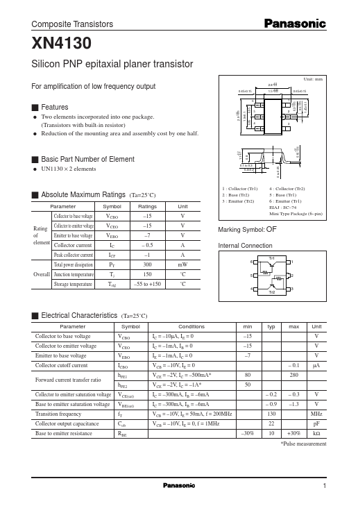
- 4±0.2 s Absolute Maximum Ratings Parameter Collector to base voltage Collector to emitter voltage Rating Emitter to base voltage of element Collector current Peak collector current Total power dissipation Overall Junction temperature Storage temperature Symbol VCBO VCEO VEBO IC ICP PT Tj Tstg (Ta=25˚C) Ratings -15 -15 -7 - 0.5 -1 300 150 -55 to +150 Unit V V V A A mW ˚C ˚C 1 : Collector (Tr1) 2 : Base (Tr2) 3 : Emitter (Tr2) 4 : Collector (Tr2) 5 : Base (Tr1) 6 : Emitter (Tr1) EIAJ : SC-74 Mini Type Package (6-pin) Marking Symbol: OF Internal Connection 6 5 4 Tr1 1 2 3 Tr2 s Electrical Characteristics Parameter Collector to base voltage Collector to emitter voltage Emitter to base voltage Collector cutoff current Forward current transfer ratio Collector to emitter saturation voltage Base to emitter saturation voltage Transition frequency Collector output capacitance Base to emitter resistance (Ta=25˚C) Symbol VCBO VCEO VEBO ICBO hFE1 hFE2 VCE(sat) VBE(sat) fT Cob RBE Conditions IC = -10µA, IE = 0 IC = -1mA, IB = 0 IE = -1mA, IC = 0 VCB = -10V, IE = 0 VCE = -2V, IC = -500mA* VCE = -2V, IC = -1A* IC = -300mA, IB = -6mA IC = -300mA, IB = -6mA VCB = -10V, IE = 50mA, f = 200MHz VCB = -10V, IE = 0, f = 1MHz -30% 80 50 - 0.2 - 0.9 130 22 10 +30% - 0.3 -1.3 V V MHz pF kΩ min -15 -15 -7 - 0.1 280 typ max Unit V V V µA 0 to 0.05 UN1130 × 2 elements
- 1 to 0.3
- Pulse measurement
- 16-0.06 +0.2 +0.1
- 45±0.1 +0.1 +0.1 1 Composite Transistors PT - Ta 500 300 XN4130 hFE - IC Collector to emitter saturation voltage VCE(sat) (V) VCE= -10V -10 VCE(sat) - IC IC/IB=10 Total power dissipation PT (mW) Forward current transfer ratio hFE 400 250 Ta=75˚C 200 25˚C -1 300 150 -25˚C 200 100 -0.1 Ta=75˚C -25˚C -0.01 -1 25˚C 100 50