XP6215
Key Features
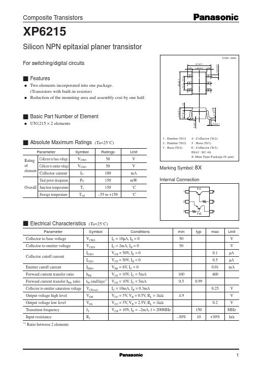
- 65 1 2 3 6 5 4
- 9±0.1 s Basic Part Number of Element q 0 to 0.1 UN1215 × 2 elements 1 : Emitter (Tr1) 2 : Emitter (Tr2) 3 : Base (Tr2)
- 7±0.1
- 2±0.1 s Absolute Maximum Ratings Parameter Rating Collector to base voltage of Collector to emitter voltage element Collector current Total power dissipation Overall Junction temperature Storage temperature Symbol VCBO VCEO IC PT Tj Tstg (Ta=25˚C) Ratings 50 50 100 150 150 -55 to +150 Unit V V mA mW ˚C ˚C 4 : Collector (Tr2) 5 : Base (Tr1) 6 : Collector (Tr1) EIAJ : SC-88 S-Mini Type Package (6-pin) Marking Symbol: 8X Internal Connection 1 2 3 Tr1 6 5 4 Tr2 s Electrical Characteristics Parameter Collector to base voltage Collector to emitter voltage Collector cutoff current Emitter cutoff current Forward current transfer ratio Forward current transfer hFE ratio Collector to emitter saturation voltage Output voltage high level Output voltage low level Transition frequency Input resistance
- 1 (Ta=25˚C) Symbol VCBO VCEO ICBO ICEO IEBO hFE hFE (small/large)*1 VCE(sat) VOH VOL fT R1 Conditions IC = 10µA, IE = 0 IC = 2mA, IB = 0 VCB = 50V, IE = 0 VCE = 50V, IB = 0 VEB = 6V, IC = 0 VCE = 10V, IC = 5mA VCE = 10V, IC = 5mA IC = 10mA, IB = 0.3mA VCC = 5V, VB = 0.5V, RL = 1kΩ VCC = 5V, VB = 2.5V, RL = 1kΩ VCB = 10V, IE = -2mA, f = 200MHz -30% 150 10 +30% 4.9 0.2 160 0.5 0.99 0.25 V V V MHz kΩ min 50 50 0.1 0.5 0.01 460 typ max Unit V V µA µA mA Ratio between 2 elements
- 12 -0.02 +0.05 1 Composite Transistors PT - Ta 250 XP6215 Total power dissipation PT (mW) 200 150 100 50