Panasonic 2SD1350
Silicon NPN Transistor
| Part No. | 2SD1350 |
|---|---|
| Datasheet | 2SD1350 Download |
| Manufacturer |  Panasonic |
| Description | Silicon NPN Transistor |
| Buy | Stock & Price |
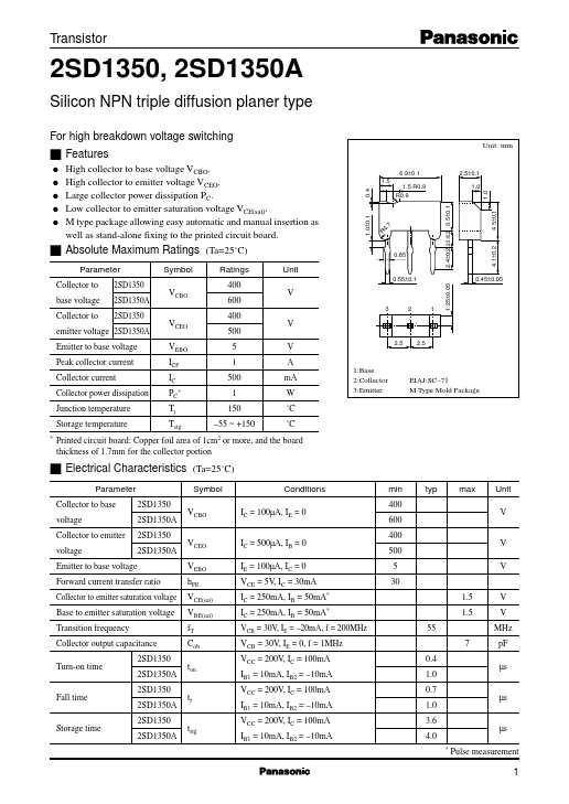
FEATURES
q q q q q Unit: mm 2.4±0.2 2.0±0.2 3.5±0.1 High collector to base voltage VCBO. High collector to emitter voltage VCEO. Large collector power dissipation PC. Low collector to emitter saturation voltage VCE(sat). M type package allowing easy automatic and manual insertion as well as stand-alone fixing to the printed circuit board. (Ta=25˚C) Ratings 400 600 400 500 5 1 500 1 150 –55 ~ +150 1cm2 Unit V 6.9±0.1 1.5 0.4 2.5±0.1 1.0 1.0 1.5 R0.9 R0.9 1.0±0.1 0.85 Parameter Collector to base voltage Collector to 2SD1350 2SD1350A 2SD1350 Symbol VCBO VCEO VEBO ICP IC PC* Tj Tstg 0.55±0.1 1.25±0.05 0.45±0.05 3 2 1 emitter voltage 2SD1350A Emitter to base voltage Peak collector current Collector current Collector power dissipation Junction temperature Storage temperature * V V A mA W ˚C ˚C 1:Base 2:Collector 3:Emitter 2.5 2.5 EIAJ:SC–71 M Type Mold Package Printed circuit board: Copper foil area of thickness of 1.7mm for the collector portion or more, and the board s Electrical Character...