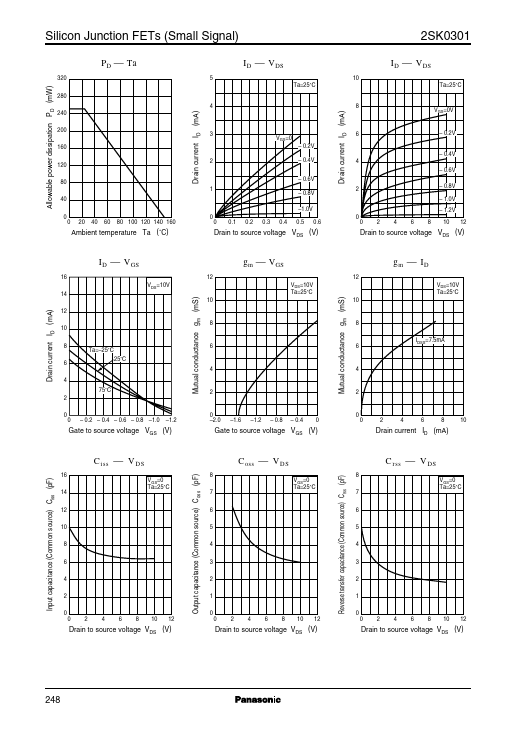
Panasonic 2SK0301
Silicon N-Channel Junction FET
| Part No. | 2SK0301 |
|---|---|
| Datasheet | 2SK0301 Download |
| Manufacturer |  Panasonic |
| Description | Silicon N-Channel Junction FET |
| Buy | Stock & Price |
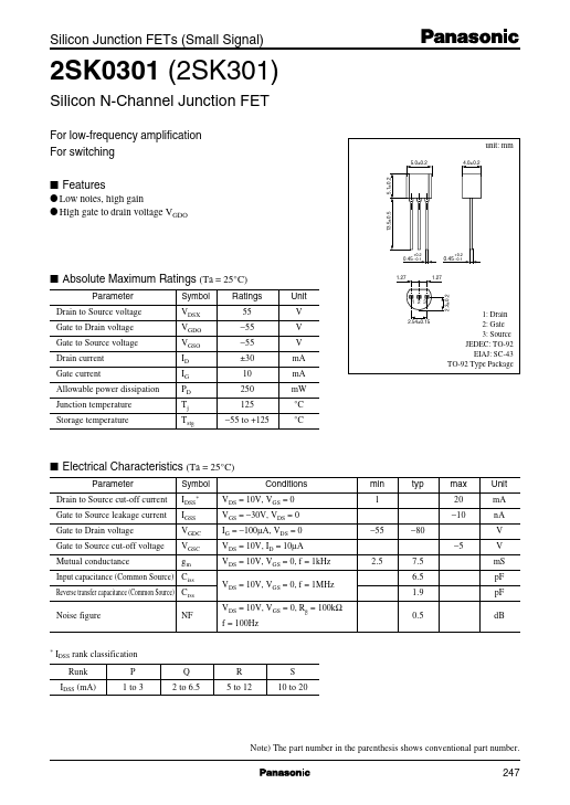
FEATURES
13.5±0.5 G Low noies, high gain G High gate to drain voltage VGDO 0.45 –0.1 +0.2 0.45 –0.1 +0.2 IABSOLUTE MAXIMUM RATINGS
(Ta = 25°C) Parameter Drain to Source voltage Gate to Drain voltage Gate to Source voltage Drain current Gate current Allowable power dissipation Junction temperature Storage temperature Symbol VDSX VGDO VGSO ID IG PD Tj Tstg Ratings 55 −55 −55 ±30 10 250 125 −55 to +125 Unit V V V mA mA mW °C °C 1.27 1.27 1 2 3 2.54±0.15 IELECTRICAL CHARACTERISTICS
(Ta = 25°C) Parameter Drain to Source cut-off current Gate to Source leakage current Gate to Drain voltage Gate to Source cut-off voltage Mutual conductance Symbol IDSS* IGSS VGDC VGSC gm Conditions VDS = 10V, VGS = 0 VGS = −30V, VDS = 0 IG = −100µA, VDS = 0 VDS = 10V, ID = 10µA VDS = 10V, VGS = 0, f = 1kHz VDS = 10V, VGS = 0, f = 1MHz VDS = 10V, VGS = 0, Rg = 100kΩ f = 100Hz 2.5 7.5 6.5 1.9 0.5 −55 −80 −5 min 1 typ max 20 −10 Unit mA nA V V mS pF pF dB Input capacitance (Common Source) Ciss Reverse transfer c...