Datasheet4U.com
🌙
DN8695 Datasheet | Panasonic
Part:
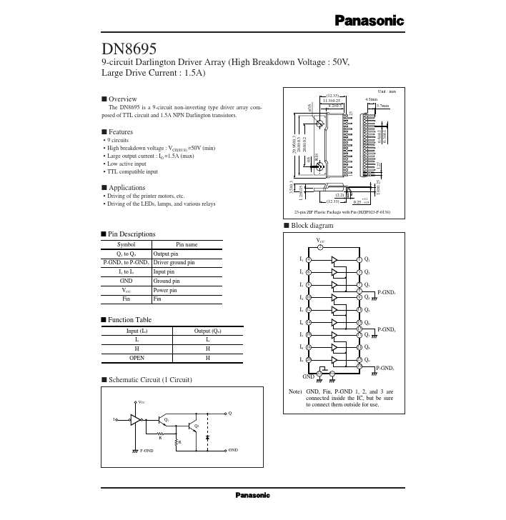
DN8695
Description:
9-circuit Darlington Driver Array
Manufacturer:
Panasonic
Size:
30.38 KB
DN8695 Datasheet (PDF) Download
Related DN8695 Datasheets
DN8690 4-circuit Darlington Driver Array
Panasonic
DN8695
Key Features
High breakdown voltage : VCE(SUS) =50V (min)
Large output current : IO =1.5A (max)
×
Close