Datasheet4U Logo Datasheet4U.com

MN673274 - Signal-Processing LSI for Multimedia Camera

Datasheet Summary

Description

Pin No.

1 2 3 4 5 6 7 8 9 10 11 12 13 14 15 16 17 18 19 20 21 22 23 24 25 26 27 Pin Name N.C.

V4 V3 VSS5 VDD5 V2 N.C.

Features

  • Input: Analog signal (A/D converter input).
  • Output: Digital output YUV signal: 8 bits Analog outputs Y signal C signal Composite video output RGB outputs.
  • Operating supply voltage: 3.3 V ± 0.3 V.
  • Operating frequency: 9.5 MHz to 28.7 MHz.
  • Main functions.
  • 10-bit A/D converter.
  • 10-bit D/A converter.
  • 2-channel 8-bit D/A converter.
  • Support for analog AGC (NN2038, NN2039).
  • CG and SSG functions.
  • 510H and.

📥 Download Datasheet

Datasheet preview – MN673274

Datasheet Details

Part number MN673274
Manufacturer Panasonic
File Size 92.62 KB
Description Signal-Processing LSI for Multimedia Camera
Datasheet download datasheet MN673274 Datasheet
Additional preview pages of the MN673274 datasheet.
Other Datasheets by Panasonic

Full PDF Text Transcription

Click to expand full text
Video Camera LSI MN673274 Signal-Processing IC for Multipurpose Cameras s Overview 
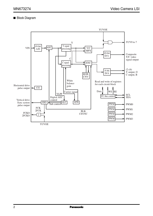
The MN673274 is designed for surveillance and PC input cameras. In addition to the basic functions of luminance signal and chrominance signal processing, it also integrates microcontroller functions (ALC, AWB, and AGC) and SSG, CG, and I2C-bus circuits on a single chip. s Features • Input: Analog signal (A/D converter input) • Output: Digital output YUV signal: 8 bits Analog outputs Y signal C signal Composite video output RGB outputs • Operating supply voltage: 3.3 V ± 0.3 V • Operating frequency: 9.5 MHz to 28.
Published: |