FEATURES
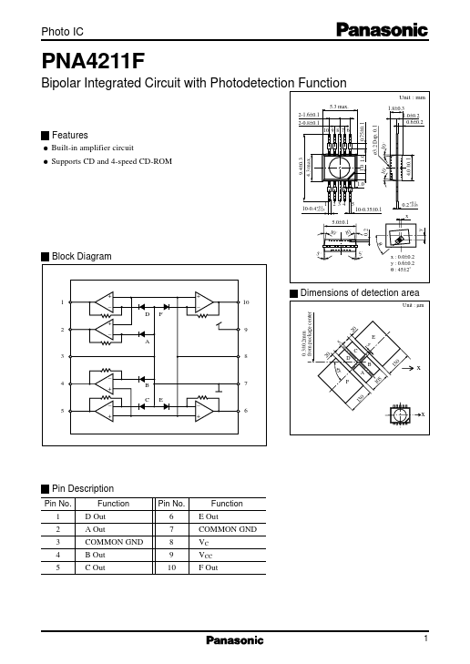
Built-in amplifier circuit 9.4±0.3 4.3 max. 10 9 8 7 6 ø3.2 Dep. 0.1 10˚ Supports CD and 4-speed CD-ROM 1.0 1 10-0.4 +0.1 –0.15 2 34 5.0±0.1 10˚ 5 10-0.35±0.1 0.2 +0.1 –0.05 x 4.0 ±0.1 x : 0.0±0.2 y : 0.6±0.2 θ : 45±2˚ Unit : µm 10˚ 10˚ 0.2 Block Diagram 5˚ 5˚ + 1 – D + 2 – A 3 – 4 + – 5 + B C E F + – 10 Dimensions of detection area 0.3±0.2mm from package center 9 20 E 5 C 8 20 D B F 13 0 A x 7 – + 6 13 0 10 5 Pin DESCRIPTION
Pin No. 1 2 3 4 5 Function D Out A Out COMMON GND B Out C Out Pin No. 6 7 8 9 10 Function E Out COMMON GND VC VCC F Out y θ 5 45˚ x 1 Photo IC PNA4211F ABSOLUTE MAXIMUM RATINGS
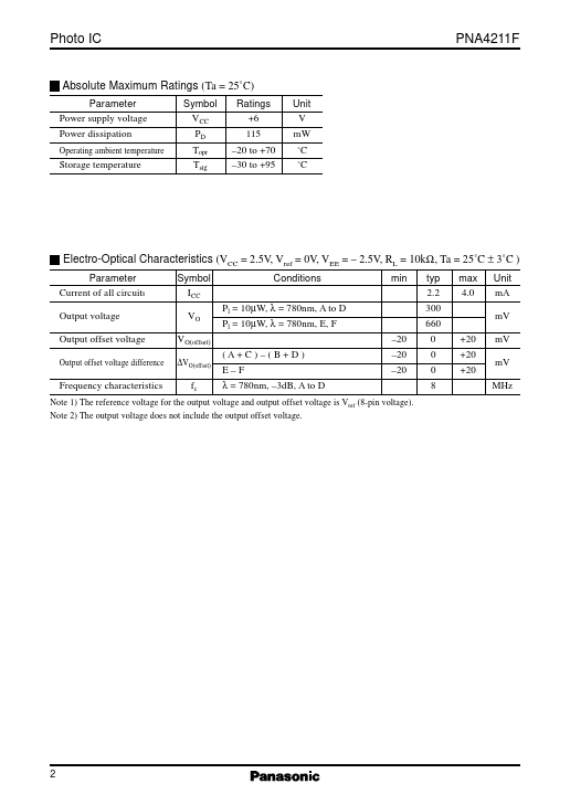
(Ta = 25˚C) Parameter Power supply voltage Power dissipation Operating ambient temperature Storage temperature Symbol VCC PD Topr Tstg Ratings +6 115 –20 to +70 –30 to +95 Unit V mW ˚C ˚C Electro-Optical Characteristics (VCC = 2.5V, Vref = 0V, VEE = – 2.5V, RL = 10kΩ, Ta = 25˚C ± 3˚C ) Parameter Current of all circuits Output voltage Output offset voltage Output offset voltage diff... Panasonic