PI5A4765
PI5A4765 is CSP Low Voltage Dual SPDT Audio Clickless Analog Switch manufactured by pSemi.
Features
- -
- -
- -
- -
- - CMOS Technology for Bus and Analog Applications Low On-Resistance: 0.6Ω @ 2.7V. Wide VCC Range: 1.65V to 5.5V Rail-to-Rail Signal Range Control Input Overvoltage Tolerance: 5.5V min. High Off Isolation: -50d B Crosstalk Rejection Reduces Signal Distortion: -80d B Break-Before-Make Switching Extended Industrial Temperature Range:
- 40°C to 85°C Packaging (Pb-free & Green available): -12-ball CSP
Description
Peri Semiconductors PI5A4765 is a dual high-bandwidth, fast single-pole double throw (SPDT) CMOS switch. It can be used as an analog switch or as a low-delay bus switch. Specified over a wide operating power supply voltage, 1.65V to 5.5V, the PI5A4765 has a low On-Resistance of 0.6Ω @ 2.7V. Break-before-make switching prevents both switches being enabled simultaneously. This eliminates signal disruption during switching. The control input, INX, tolerates input drive signals up to 6.0V, independent of supply voltage. The PI5A4765 offers a headphone & mute detection function through utilization of an on-chip parator. When the negative terminal of the parator (P-) is less than the threshold (internally set to VCC/3, P0 (parator output) is a logic high. A logic low on P0 occurs when P- rises above the the threshold. PI5A4765 also offers shunt switches connected to ground in order to dissipate capacitance that builds up on the unconnected NC or NO line. As a result, reduction of popping and clicking sounds is achieved when switching between audio sources.
Applications
- Cell Phones
- PDAs
- MP3 players
- Portable Instrumentation
- puter Peripherals
- Speaker Headset Switching
- Power Routing
- Relay Replacement
- Audio/Video Signal Routing
- PCMCIA Cards
- Modems
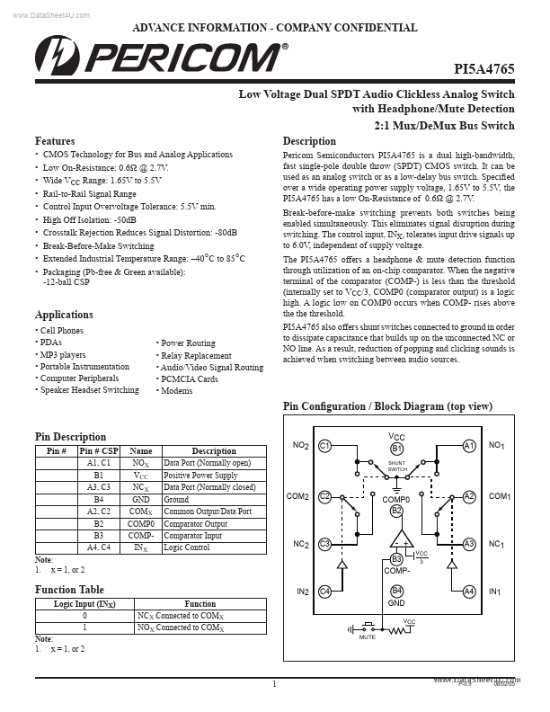
Pin Configuration / Block Diagram (top view) Pin Description
Pin # Pin # CSP
A1, C1 B1 A3, C3 B4 A2, C2 B2 B3 A4, C4 Note: 1. x = 1, or 2
VCC B1
SHUNT SWITCH
Name
NOX VCC NCX GND X P0 PINX
Description
Data Port (Normally open) Positive Power Supply Data Port (Normally closed)...