PI74ALVCH16260
PI74ALVCH16260 is 12-Bit To 24-Bit Multiplexed D-Type Latch manufactured by Pericom Semiconductor.
Description
Product Features
PI74ALVCH16260 is designed for low voltage operation VCC = 2.3V to 3.6V Hysteresis on all inputs Typical VOLP (Output Ground Bounce) < 0.8V at VCC = 3.3V, TA = 25°C ..
- Typical VOHV (Output VOH Undershoot) < 2.0V at VCC = 3.3V, TA = 25°C
- Bus Hold retains last active bus state during 3-State, eliminating the need for external pullup resistors
- Industrial operation at 40°C to +85°C
- Packages available: 56-pin 240 mil wide plastic TSSOP (A) 56-pin 300 mil wide plastic SSOP (V)
- -
- -
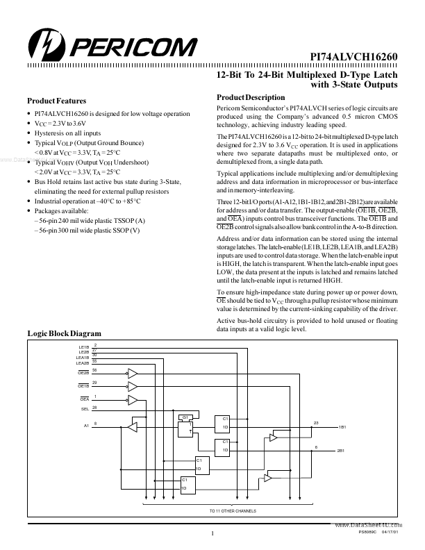
Peri Semiconductors PI74ALVCH series of logic circuits are produced using the panys advanced 0.5 micron CMOS technology, achieving industry leading speed. The PI74ALVCH16260 is a 12-bit to 24-bit multiplexed D-type latch designed for 2.3V to 3.6 VCC operation. It is used in applications where two separate datapaths must be multiplexed onto, or demultiplexed from, a single data path. Typical applications include multiplexing and/or demultiplexing address and data information in microprocessor or bus-interface and in memory-interleaving. Three 12-bit I/O ports (A1-A12, 1B1-1B12, and 2B1-2B12) are available for address and/or data transfer. The output-enable (OE1B, OE2B, and OEA) inputs control bus transceiver functions. The OE1B and OE2B control signals also allow bank control in the A-to-B direction. Address and/or data information can be stored using the internal storage latches. The latch-enable (LE1B, LE2B, LEA1B, and LEA2B) inputs are used to control data storage. When the latch-enable input is HIGH, the latch is transparent. When the latch-enable input goes LOW, the data present at the inputs is latched and remains latched until the latch-enable input is returned HIGH. To ensure high-impedance state during power up or power down, OE should be tied to VCC through a pullup resistor whose minimum value is determined by the current-sinking capability of the driver.
Logic Block Diagram
LE1B 2 LE2B 27 30 LEA1B LEA2B 55 OE2B OE1B OEA
56 29
Active...