Datasheet4U Logo Datasheet4U.com

PI49FCT20803 - (PI49FCT20802 / PI49FCT20803) 1:5/1:7 2.5V Clock Buffer

Download the PI49FCT20803 datasheet PDF. This datasheet also covers the PI49FCT20802 variant, as both devices belong to the same (pi49fct20802 / pi49fct20803) 1:5/1:7 2.5v clock buffer family and are provided as variant models within a single manufacturer datasheet.

General Description

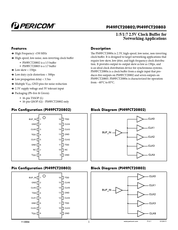
The PI49FCT2080x is 2.5V, high-speed, low noise, non-inverting clock buffer.

It is designed to target networking applications that require low-skew, low-jitter, and high-frequency clock distribution.

Key Features

  • ÎÎHigh Frequency >150 MHz ÎÎHigh-speed, low-noise, non-inverting clock buffer àà PI49FCT20802 is a 1:5 buffer àà PI49FCT20803 is a 1:7 buffer ÎÎLow skew < 150ps ÎÎLow duty cycle distortion < 300ps ÎÎLow propagation delay < 3.5ns ÎÎMultiple VDD, GND pins for noise reduction ÎÎ2.5V supply voltage and 3V tolerant input ÎÎPackaging (Pb-free & Green): àà 16-pin TSSOP (L) àà 16-pin QSOP (Q) - PI49FCT20802 only Pin Configuration (PI49FCT20802) BUF_IN 1 GND 2 CLK0 3 VDD 4 CLK1 5 GND 6 NC 7 VDD 8 16 VD.

📥 Download Datasheet

Note: The manufacturer provides a single datasheet file (PI49FCT20802_PericomSemiconductor.pdf) that lists specifications for multiple related part numbers.

Full PDF Text Transcription (Reference)

The following content is an automatically extracted verbatim text from the original manufacturer datasheet and is provided for reference purposes only.

View original datasheet text
Features ÎÎHigh Frequency >150 MHz ÎÎHigh-speed, low-noise, non-inverting clock buffer àà PI49FCT20802 is a 1:5 buffer àà PI49FCT20803 is a 1:7 buffer ÎÎLow skew < 150ps ÎÎLow duty cycle distortion < 300ps ÎÎLow propagation delay < 3.5ns ÎÎMultiple VDD, GND pins for noise reduction ÎÎ2.5V supply voltage and 3V tolerant input ÎÎPackaging (Pb-free & Green): àà 16-pin TSSOP (L) àà 16-pin QSOP (Q) - PI49FCT20802 only Pin Configuration (PI49FCT20802) BUF_IN 1 GND 2 CLK0 3 VDD 4 CLK1 5 GND 6 NC 7 VDD 8 16 VDD 15 CLK4 14 CLK3 13 GND 12 CLK2 11 VDD 10 NC 9 GND Pin Configuration (PI49FCT20803) BUF_IN 1 GND 2 CLK0 3 VDD 4 CLK1 5 GND 6 CLK2 7 VDD 8 11-0004 16 VDD 15 CLK6 14 CLK5 13 GND 12 CLK4 11 VDD 10 CLK3 9 GND PI49FCT20802/PI49FCT20803 1:5/1:7 2.