Datasheet Summary
Features
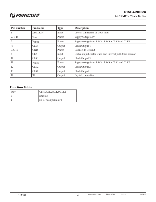
ÎÎSupport XTAL or Clock input at 24MHz ÎÎFour buffered outputs support VDDO operation ÎÎVery low phase jitter(RMS) : < 1.5ps (max) ÎÎVery low additive jitter: <300fs (typ) ÎÎ3.3V supply voltage for Core ÎÎ1.8V ~ 3.3V supply voltage for two output banks ÎÎPackaging: 16-pin TSSOP ÎÎmercial & Industrial Temperature support
Applications
ÎÎNetworking Systems ÎÎFemtocell BTS ÎÎPeripheral
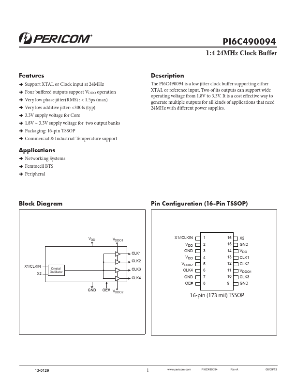
Block Diagram
1:4 24MHz Clock Buffer
Description
The PI6C490094 is a low jitter clock buffer supporting either XTAL or reference input. Two of its outputs can support wide operating voltage from 1.8V to 3.3V. It is a cost effective way to generate multiple outputs for all kinds of...