Datasheet Summary
Features
ÎÎLow skew outputs (250 ps) ÎÎPackaged in 8-pin SOIC ÎÎLow power CMOS technology ÎÎOperating Voltages of 1.5 V to 3.3 V ÎÎOutput Enable pin tri-states outputs ÎÎ3.6 V tolerant input clock ÎÎIndustrial temperature ranges
Low Skew 1 TO 4 Clock Buffer
Description
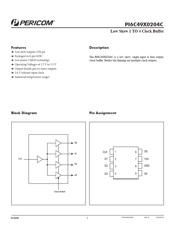
The PI6C49X0204C is a low skew, single input to four output, clock buffer. Perfect for fanning out multiple clock outputs.
Block Diagram
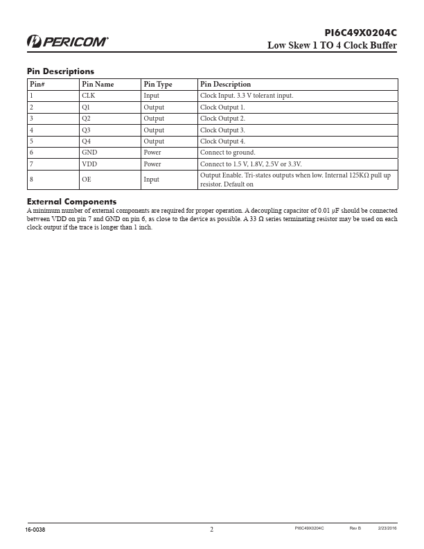
Pin Assignment
CLK 16-0038
Q0 Q1 Q2 Q3
Output Enable
CLK 1 Q1 2 Q2 3 Q3 4
8 OE 7 VDD 6 GND 5 Q4
1 PI6C49X0204C
Rev B
2/23/2016
PI6C49X0204C Low Skew 1 TO 4 Clock Buffer
Pin Descriptions
Pin# 1 2 3 4 5 6 7
Pin Name CLK Q1 Q2 Q3 Q4 GND VDD
8 OE
Pin Type Input...