Pericom Semiconductor PI6C2502
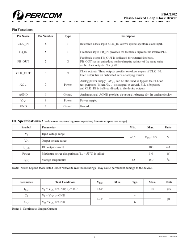
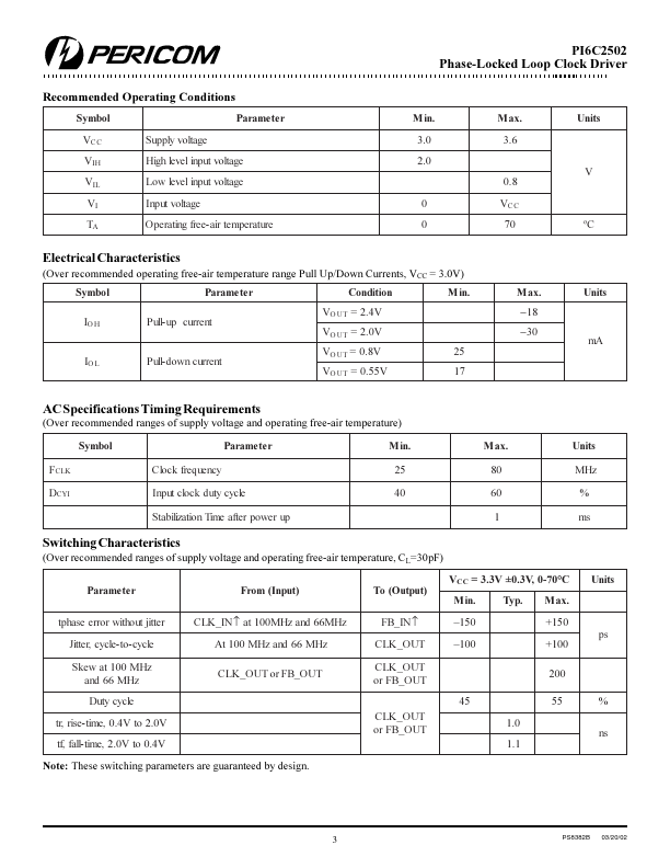
The PI6C2502 features a low-skew, low-jitter, phase-locked loop (PLL) clock driver. By connecting the feedback FB_OUT output to the feedback FB_IN input, the propagation delay from the CLK_IN input to any clock output will be nearly zero. The device-to-device skew introduced can significantly reduce the performance.| Part No. | PI6C2502 |
|---|---|
| Datasheet | PI6C2502 Download |
| Manufacturer |  Pericom Semiconductor |
| Description | Phase-Locked Loop Clock Driver |
| Buy | Stock & Price |
FEATURES
● High-Performance Phase-Locked-Loop Clock Distribution for Networking,● Synchronous DRAM modules for server/workstation/ PC applications
● Allows Clock Input to have Spread Spectrum modulation for EMI reduction
● Zero Input-to-Output delay
● Low jitter: Cycle-to-Cycle jitter ±100ps max.
● On-chip series damping resistor at clock output drivers for low noise and EMI reduction
● Operates at 3.3V VCC
● Wide range of Clock Frequencies up to 80 MHz
● Package: Plastic 8-pin SOIC Package (W) Product
DESCRIPTION
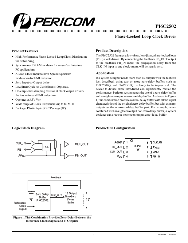
Application If a system designer needs more than 16 outputs with the features just described, using two or more zero-delay buffers such as PI6C2509Q, and PI6C2510Q, is likely to be impractical. Pericom recommends the use of a zero-delay buffer and an eighteen output non-zero-delay buffer. As shown in Figure 1, this combination produces a zero-delay buffer with all the signal characteristics of the original zero-delay buffer, but with as many outputs as the non-zero-delay buffer part.