Pericom Semiconductor PI6C49003A
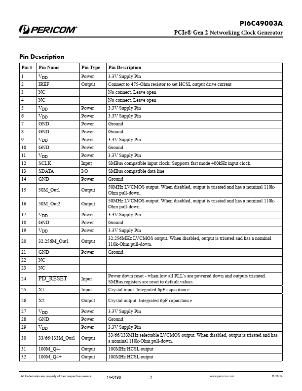
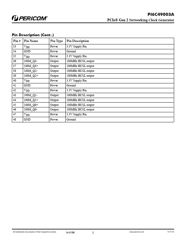
The PI6C49003A is a clock generator device intended for PCIe® Gen2 networking applications. The device includes five 100MHz differential Host Clock Signal Level (HCSL) outputs for PCIe Gen 2, two single-ended 50MHz outputs, one single-ended 32.256MHz output, and one selectable single-ended 33/66/133MHz output. Using a serially programmable SMBUS interface, the PI6C49003A incorporates spread spectrum modulation on the twelve 100MHz HCSL PCIe Gen 2 outputs, and independent frequency margining on the 50MHz output, 33.3333MHz and 66.6666MHz clock outputs.| Part No. | PI6C49003A |
|---|---|
| Datasheet | PI6C49003A Download |
| Manufacturer |  Pericom Semiconductor |
| Description | Gen 2 Networking Clock Generator |
| Buy | Stock & Price |
FEATURES
● 3.3V +/-10% Supply Voltage● Uses 25MHz xtal
● Five PCIe® Gen. 2 100MHz HCSL outputs with optional -0.5% spread spectrum support
● Two LVCMOS 50MHz outputs that support +/- 10% frequency margining
● One frequency selectable 33/66/133MHz LVCMOS output
● One 32.256MHz LVCMOS output
● Industrial temperature -40°C to 85°C
● Package: 48-pin TSSOP package
DESCRIPTION
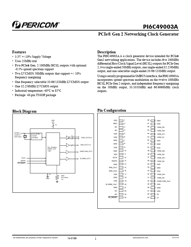
Block Diagram 25 MHz crystal or clock input Clock Buffer/ Crystal Oscillator VDD 14 SCLK SDATA PD_RESET PLL, Dividers, Buffers, and Logic 5 10 GND ISET 475 Ohms 1% Pin Configuration 100M_OUT(0-4) 50M_OUT(1-2) 33/66/133M_OUT1 32.256M_OUT1 VDD IREF NC NC VDD VDD GND GND VDD GND VDD SCLK SDATA GND 50M_Out1 50M_Out2 VDD GND VDD 32.256M_Out1 GND NC NC PD_RESET 1 2 3 4 5 6 7 8 9 10 11 12 13 14 15 16 17 18 19 20 21 22 23 24 48 GND 47 VDD 46 100M_Q045 100M_Q0+ 44 100M_Q1+ 43 100M_Q142 VDD 41 GND 40 VDD 39 100M_Q2+ 38 100M_Q237 100M_Q3+ 36 100M_Q335 VDD 34 GND 33 VDD 32 100M_Q4+ 31 100M_Q430 33/66/133M_Out1 29 VDD 28 GND 27 VDD 26 X2 25 X1 All trademarks are property of their respective owners.