Pericom Semiconductor PI74SSTU32864A
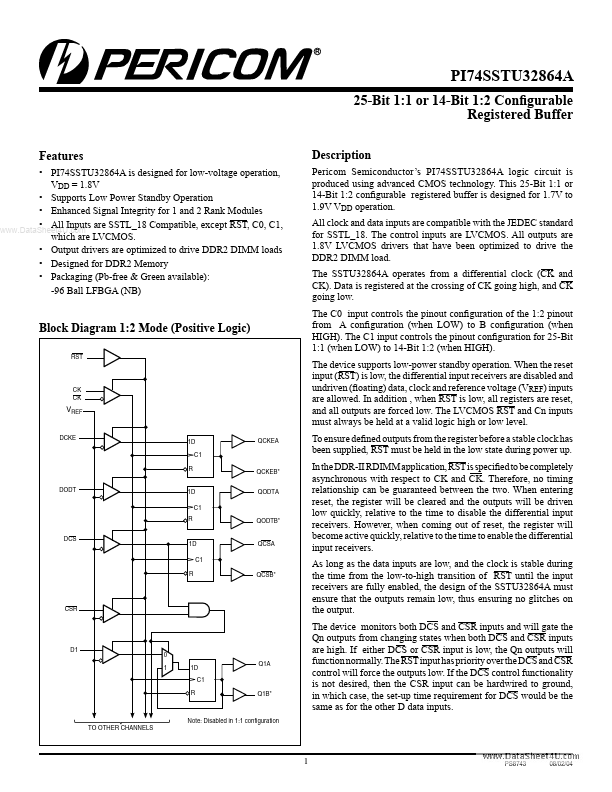
PI74SSTU32864A is designed for low-voltage operation, VDD = 1.8V • Supports Low Power Standby Operation • Enhanced Signal Integrity for 1 and 2 Rank Modules • All Inputs are SSTL_18 Compatible, except RST, C0, C1, which are LVCMOS. This 25-Bit 1:1 or 14-Bit 1:2 configurable registered buffer is designed for 1.7V to 1.9V VDD operation. The control inputs are LVCMOS.| Part No. | PI74SSTU32864A |
|---|---|
| Datasheet | PI74SSTU32864A Download |
| Manufacturer |  Pericom Semiconductor |
| Description | 25-Bit 1:1 or 14-Bit 1:2 Configurable Registered |
| Buy | Stock & Price |
FEATURES
●● Output drivers are optimized to drive DDR2 DIMM loads
● Designed for DDR2 Memory
● Packaging (Pb-free & Green available): -96 Ball LFBGA (NB)
DESCRIPTION
Pericom Semiconductor’s PI74SSTU32864A logic circuit is produced using advanced CMOS technology. All clock and data inputs are compatible with the JEDEC standard for SSTL_18. The control inputs are LVCMOS. All outputs are 1.8V LVCMOS drivers that have been optimized to drive the DDR2 DIMM load. The SSTU32864A operates from a differential clock (CK and CK). Data is registered at the crossing of CK going high, and CK going low. The C0 input controls the pinout configuration of the 1:2 pinout from A configuration (when LOW) to B configuration (when HIGH). The C1 input controls the pinout configuration for 25-Bit 1:1 (when LOW) to 14-Bit 1:2 (when HIGH). The device supports low-power standby operation. When the reset input (RST) is low, the differential input receivers are disabled and undriven (floating) data, clock and reference voltage (VREF) inputs are allowed.
