FEATURES
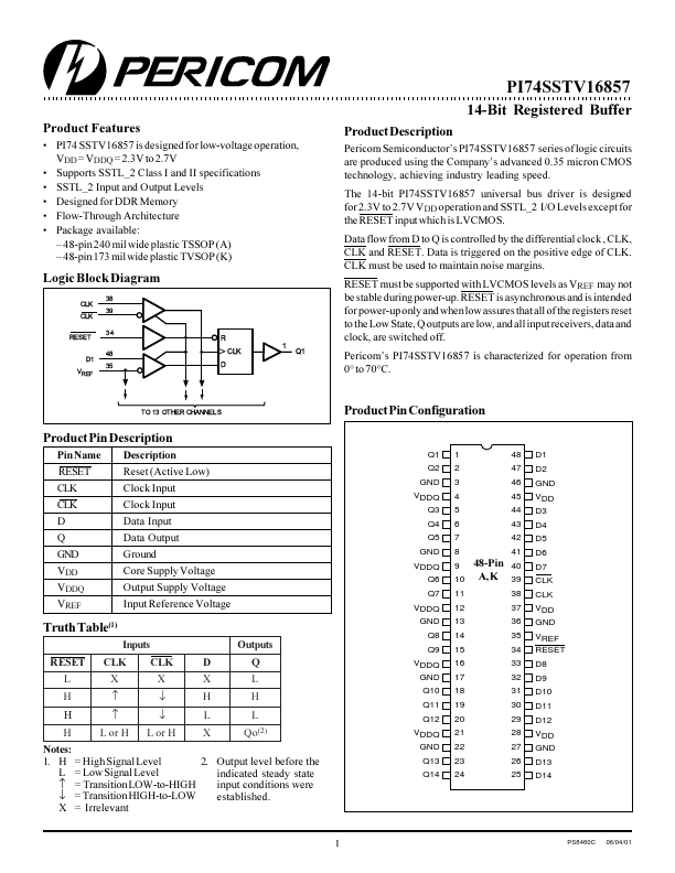
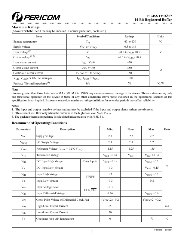
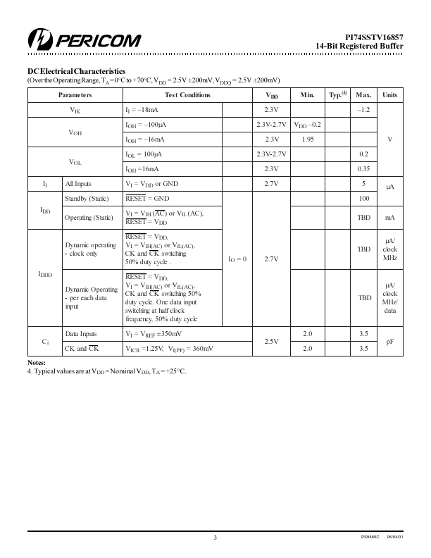
PI74 SSTV16857 is designed for low-voltage operation, VDD = VDDQ = 2.3V to 2.7V Supports SSTL_2 Class I and II specifications SSTL_2 Input and Output Levels Designed for DDR Memory Flow-Through Architecture Package available: 48-pin 240 mil wide plastic TSSOP (A) 48-pin 173 mil wide plastic TVSOP (K) Product DESCRIPTION
Pericom Semiconductors PI74SSTV16857 series of logic circuits are produced using the Companys advanced 0.35 micron CMOS technology, achieving industry leading speed. The 14-bit PI74SSTV16857 universal bus driver is designed for 2.3V to 2.7V VDD operation and SSTL_2 I/O Levels except for the RESET input which is LVCMOS. Data flow from D to Q is controlled by the differential clock , CLK, CLK and RESET. Data is triggered on the positive edge of CLK. CLK must be used to maintain noise margins. RESET must be supported with LVCMOS levels as VREF may not be stable during power-up. RESET is asynchronous and is intended for power-up only and when low assures that all of the registers reset to the Low State, Q outputs are low, and all input receivers, data and clock, are switched off. Pericom Semiconductor