PL611S-26
PL611S-26 is PicoPLLTM Programmable Clock manufactured by PhaseLink Corporation.
(Preliminary)
1.8V-3.3V Pico PLL TM Programmable Clock
Features
- Advanced One Time Programmable (OTP) PLL design
- Programmable PLL or direct oscillation operation
- Very low Jitter and Phase Noise (30-70ps Pk-Pk typical)
- Output Frequency up to o 133MHz @ 1.8V operation o 166MHz @ 2.5V operation o 200MHz @ 3.3V operation ..
- Reference Input Frequency: 1MHz to 200MHz
- Accepts >0.1V reference signal input voltage
- Low current consumption, <10µA when PDB is activated
- One programmable I/O pin can be configured as Output Enable (OE),Power Down (PDB) input or an additional clock output (CLK1).
- Frequency Switching (FSEL) capability
- Single 1.8V, 2.5V, or 3.3V ± 10% power supply
- Operating temperature range from -40 ° C to 85 ° C
- Available in 6-pin SOT23 and DFN GREEN/Ro HS pliant packaging
DESCRIPTION
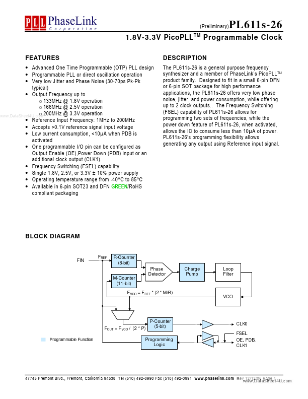
The PL611s-26 is a general purpose frequency synthesizer and a member of Phase Link’s Pico PLL TM product family. Designed to fit in a small 6-pin DFN or 6-pin SOT package for high performance applications, the PL611s-26 offers very low phase noise, jitter, and power consumption, while offering up to 2 clock outputs.. The Frequency Switching (FSEL) capability of PL611s-26 allows for programming two sets of frequencies, while the power down feature of PL611s-26, when activated, allows the IC to consume less than 10µA of power. PL611s-26’s programming flexibility allows generating any output using Reference input signal.
BLOCK DIAGRAM
FREF
R-Counter (8-bit) M-Counter (11-bit) Phase Detector Charge Pump Loop Filter
F VCO = F REF
- (2
- M/R)
FOUT = F VCO / (2
- P)
Programmable Function
P-Counter (5-bit)
CLK0 FSEL
Programming Logic
OE, PDB,...