PL611S-28
PL611S-28 is PicoPLLTM Programmable Clock manufactured by PhaseLink Corporation.
(Preliminary)
1.8V-3.3V Pico PLL TM , World’s Smallest Programmable Clock
Features
- Designed for Very Low-Power applications
- Offered in Tiny GREEN /Ro HS pliant packages o 6-pin DFN (2.0mmx1.3mmx0.6mm) o 6-pin SC70 (2.3mmx2.25mmx1.0mm) o 6-pin SOT23 (3.0mmx3.0mmx1.35mm)
- Input Frequency: o Fundamental Crystal: 10MHz to 50MHz o Reference Input: 1MHz to 200MHz
- Accepts >0.1V reference signal input voltage ..
- Output Frequency: o <65MHz @ 1.8V operation o <90MHz @ 2.5V operation o <125MHz @ 3.3V operation
- Disabled outputs programmable as Hi Z or Active Low.
- Low current consumption: o <1.2m A @ 27MHz o < 5µA when PDB is activated
- Single 1.8V, 2.5V, or 3.3V ± 10% power supply
- Operating temperature range from -40 ° C to 85 ° C
DESCRIPTION
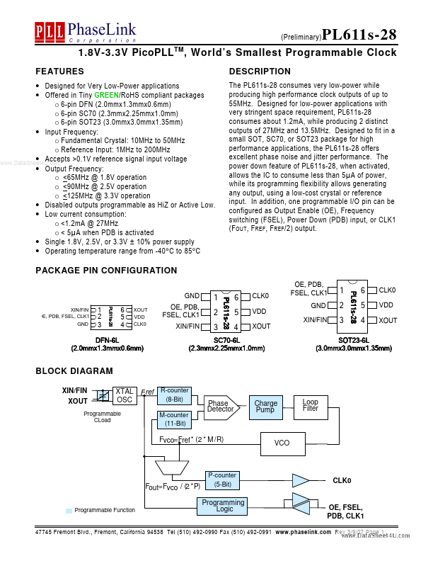
The PL611s-28 consumes very low-power while producing high performance clock outputs of up to 55MHz. Designed for low-power applications with very stringent space requirement, PL611s-28 consumes about 1.2m A, while producing 2 distinct outputs of 27MHz and 13.5MHz. Designed to fit in a small SOT, SC70, or SOT23 package for high performance applications, the PL611s-28 offers excellent phase noise and jitter performance. The power down feature of PL611s-28, when activated, allows the IC to consume less than 5µA of power, while its programming flexibility allows generating any output, using a low-cost crystal or reference input. In addition, one programmable I/O pin can be configured as Output Enable (OE), Frequency switching (FSEL), Power Down (PDB) input, or CLK1 (F OUT , F REF , F REF /2) output.
PACKAGE PIN CONFIGURATION
XIN/FIN OE, PDB, FSEL, CLK1 GND
1 2 3
6 5 4
CLK0 VDD XOUT
OE, PDB, FSEL, CLK1 GND XIN/FIN
1 2 3
6 5 4
CLK0 VDD XOUT
1 2 3
6 5 4
XOUT VDD CLK0
OE, PDB, FSEL, CLK1 XIN/FIN
DFNDFN-6L (2.0mmx1 mmx1.3mmx0 mmx0.6mm) mm)
BLOCK DIAGRAM
XIN/FIN XOUT XTAL F ref R-counter (8-Bit)...