PLL103-01
PLL103-01 is Low Skew Buffer manufactured by PhaseLink Corporation.
FEATURES
Generate 18 copies of High-speed clock inputs. Supports up to four SDRAM DIMMS synchronous clocks.
- Supports 2-wire I2C serial bus interface with readback.
- 50% duty cycle with low jitter.
- Less than 5ns delay. ..
- Skew between any outputs is less than 250 ps.
- Tri-state pin for testing.
- Frequency up to 133 MHZ.
- 3.0V-3.7V Supply range.
- 48-pin SSOP package.
- -
PIN CONFIGURATION
N/C N/C VDD SDRAM0 SDRAM1 GND VDD SDRAM2 SDRAM3 GND BUF_IN VDD SDRAM4 SDRAM5 GND VDD SDRAM6 SDRAM7 GND VDD SDRAM16 GND VDD1 SDATA 1 2 3 4 5 6 7 48 47 46 45 44 43 42 41 40 39 38 37 36 35 34 33 32 31 30 29 28 27 26 25 N/C N/C VDD SDRAM15 SDRAM14 GND VDD SDRAM13 SDRAM12 GND OE^ VDD SDRAM11 SDRAM10 GND VDD SDRAM9 SDRAM8 GND VDD SDRAM17 GND GND1 SCLK
8 9 10 11 12 13 14 15 16 17 18 19 20 21 22 23 24
BLOCK DIAGRAM
SDRAM0 SDATA SCLK I2C Control SDRAM1 SDRAM2 SDRAM3 SDRAM4 SDRAM5 SDRAM6 SDRAM7 SDRAM8 BUF_IN SDRAM9 SDRAM10 SDRAM11 SDRAM12 SDRAM13 SDRAM14 SDRAM15 SDRAM16 SDRAM17 OE
Note: ^: pull up
POWER GROUP
- - VDD: SDRAM( 0:17 ) VDD1: I2C Circuitry
GROUND GROUP
- - GND: SDRAM( 0:17 ) GND1: I2C Circuitry
KEY SPECIFICATIONS
- -
- - BUFIN to SDRAM outputs Delay: 1 ~ 5 ns. Output Slew: ≥ 1.5 V/ns. Output Skew: ± 250 ps. Output Duty Cycle: 50% ± 5%.
47745 Fremont Blvd., Fremont, California 94538 TEL (510) 492-0990 FAX (510) 492-0991
Rev 03/08/00 Page 1
Low Skew Buffers
PIN DESCRIPTIONS
Name
SDRAM (0:3) SDRAM (4:7) SDRAM (8:11) SDRAM (12:15)
..
Number
4,5,8,9 13,14,17,18 31,32,35,36 40,41,44,45 21,28 38 11 24 25 3,7,12,16,20,2 9,33,37,42,46 23 6,10,15,19,22, 27,30,34,39,43 26 1,2,47,48
Type
O O O O O I I B I P P P P SDRAM Byte0 Clock outputs. SDRAM Byte1 Clock outputs. SDRAM Byte2 Clock outputs. SDRAM Byte3 Clock outputs. SDRAM Byte4 Clock outputs.
Description
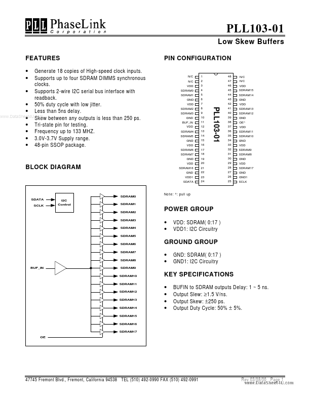
SDRAM (16:17) OE BUF_IN SDATA SCLK VDD VDD1 GND GND1 N/C
Tristates all outputs, active low. Has internal pull-up. Input for fanout buffers SDRAM (0:17). Serial data inputs for serial...