• Part: PLL103-04
  • Description: 1-to-4 Clock Distribution Buffer
  • Manufacturer: PhaseLink Corporation
  • Size: 150.92 KB
Download PLL103-04 Datasheet PDF
PhaseLink Corporation
PLL103-04
PLL103-04 is 1-to-4 Clock Distribution Buffer manufactured by PhaseLink Corporation.
FEATURES 4 outputs identical to FIN. Low skew (< 250 ps between outputs). Input / Output frequency range 0 - 160 MHz 25m A drive capability at TTL levels. 70m A drive capability at CMOS levels. Output enable mode available to tri-state all outputs. .. - 3.3V operation. - Available in 8-Pin 150mil SOIC. - - - - - - PIN CONFIGURATION FIN CLK1 CLK2 CLK3 1 8 OE^ VDD GND CLK4 2 3 4 7 6 5 FIN = 0 ~ 160 Mhz Note: ^: Internal pull-up (30k Ω ) DESCRIPTIONS 
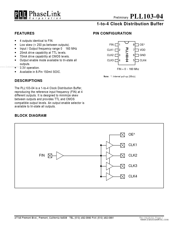
The PLL103-04 is a 1-to-4 Clock Distribution Buffer, reproducing the reference input frequency (FIN) at 4 different outputs. It is designed to minimize skew between outputs and provides TTL and CMOS patible output levels. An output enable selector is available to tri-state all outputs. BLOCK DIAGRAM OE^ CLK1 FIN CLK2 CLK3 CLK4 47745 Fremont Blvd., Fremont, California 94538 TEL (510) 492-0990 FAX (510) 492-0991 Rev 09/26/00 Page 1 Preliminary 1-to-4 Clock Distribution Buffer PIN DESCRIPTIONS Name FIN CLK1 CLK2 CLK3 CLK4 .. GND VDD OE Number 1 2 3 4 5 6 7 8 Type I O O O O P P I Buffered Clock Output. Buffered Clock Output. Buffered Clock Output. Buffered Clock Output. Ground. 3.3V Power Supply. Description Input Clock Frequency (FIN range 0 ~ 160MHz). Output Enable. Tri-states all outputs if low. Internal pull-up resistor of 30 k Ω 47745 Fremont Blvd., Fremont, California 94538 TEL (510) 492-0990 FAX (510) 492-0991 Rev 09/26/00 Page 2 Preliminary 1-to-4 Clock Distribution Buffer ELECTRICAL SPECIFICATIONS 1. Absolute Maximum Ratings PARAMETERS Supply Voltage Range Input Voltage Range Output Voltage .....