Datasheet4U Logo Datasheet4U.com

PLL103-06 - DDR SDRAM Buffer

General Description

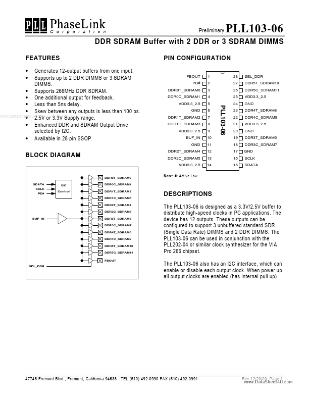
The PLL103-06 is designed as a 3.3V/2.5V buffer to distribute high-speed clocks in PC applications.

The device has 12 outputs.

These outputs can be configured to support 3 unbuffered standard SDR (Single Data Rate) DIMMS and 2 DDR DIMMS.

Key Features

  • Generates 12-output buffers from one input. Supports up to 2 DDR DIMMS or 3 SDRAM DIMMS.
  • Supports 266MHz DDR SDRAM.
  • One additional output for feedback.
  • Less than 5ns delay.
  • Skew between any outputs is less than 100 ps. www. DataSheet4U. com.
  • 2.5V or 3.3V Supply range.
  • Enhanced DDR and SDRAM Output Drive selected by I2C.
  • Available in 28 pin SSOP.
  • PIN.

📥 Download Datasheet

Datasheet Details

Part number PLL103-06
Manufacturer PhaseLink Corporation
File Size 176.96 KB
Description DDR SDRAM Buffer
Datasheet download datasheet PLL103-06 Datasheet

Full PDF Text Transcription (Reference)

The following content is an automatically extracted verbatim text from the original manufacturer datasheet and is provided for reference purposes only.

View original datasheet text
Preliminary PLL103-06 DDR SDRAM Buffer with 2 DDR or 3 SDRAM DIMMS FEATURES Generates 12-output buffers from one input. Supports up to 2 DDR DIMMS or 3 SDRAM DIMMS. • Supports 266MHz DDR SDRAM. • One additional output for feedback. • Less than 5ns delay. • Skew between any outputs is less than 100 ps. www.DataSheet4U.com • 2.5V or 3.3V Supply range. • Enhanced DDR and SDRAM Output Drive selected by I2C. • Available in 28 pin SSOP. • • PIN CONFIGURATION FBOUT PD# DDR0T_SDRAM0 DDR0C_SDRAM1 VDD3.3_2.5 GND DDR1T_SDRAM2 DDR1C_SDRAM3 VDD3.3_2.5 BUF_IN GND DDR2T_SDRAM4 DDR2C_SDRAM5 VDD3.3_2.5 DDR0T_SDRAM0 1 2 3 4 5 6 7 8 9 10 11 12 13 14 28 27 26 25 24 23 22 21 20 19 18 17 16 15 SEL_DDR DDR5T_SDRAM10 DDR5C_SDRAM11 VDD3.3_2.5 GND DDR4T_SDRAM8 DDR4C_SDRAM9 VDD3.3_2.