• Part: PLL103-07
  • Description: 2 DIMM DDR Fanout Buffer
  • Manufacturer: PhaseLink Corporation
  • Size: 175.36 KB
Download PLL103-07 Datasheet PDF
PhaseLink Corporation
PLL103-07
PLL103-07 is 2 DIMM DDR Fanout Buffer manufactured by PhaseLink Corporation.
FEATURES - Generates 12-output buffers from one input. - Supports VIA Pro266 DDR chipset. - Supports up to 2 DDR DIMMS. - Supports up to 400MHz DDR, SDRAMS. - One additional output for feedback. - 6 differential clock distribution. - Less than 5ns delay. .. - Skew between any outputs is less than 100 ps. - 2.5V Supply range. - Available in 28-pin SSOP. PIN CONFIGURATION FBOUT GND DDRT0 DDRC0 VDD2.5 GND DDRT1 DDRC1 VDD2.5 BUF_IN GND DDRT2 DDRC2 VDD2.5 DDR0T Note: #: Active Low 1 2 3 4 5 6 7 8 9 10 11 12 13 14 28 27 26 25 24 23 22 21 20 19 18 17 16 15 GND DDRT5 DDRC5 VDD2.5 GND DDRT4 DDRC4 VDD2.5 GND DDRT3 DDRC3 VDD2.5 SCLK SDATA BLOCK DIAGRAM SDATA SCLK I2C Control DDR0C DDR1T DDR1C DDR2T DDR2C DESCRIPTIONS 
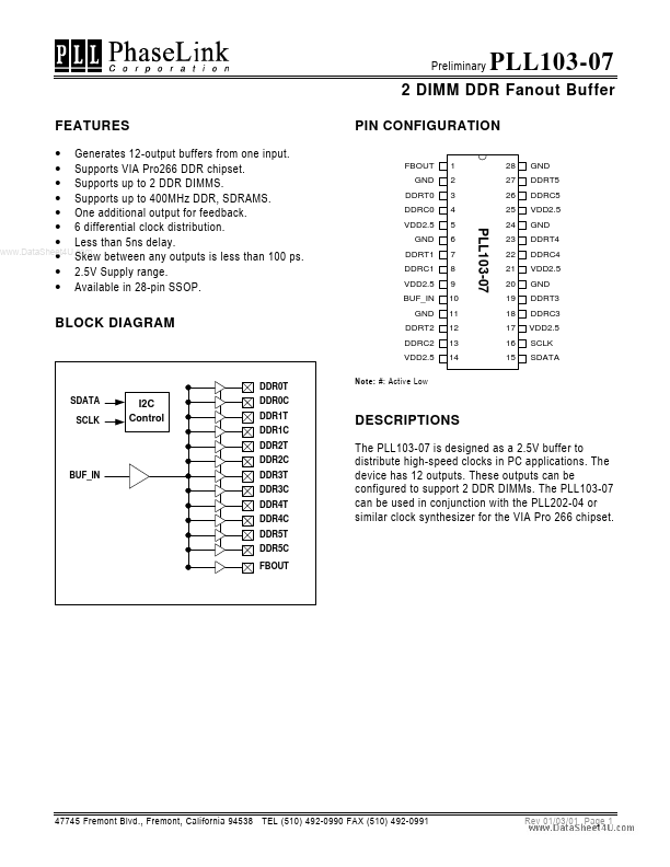
The PLL103-07 is designed as a 2.5V buffer to distribute high-speed clocks in PC applications. The device has 12 outputs. These outputs can be configured to support 2 DDR DIMMs. The PLL103-07 can be used in conjunction with the PLL202-04 or similar clock synthesizer for the VIA Pro 266 chipset. BUF_IN DDR3T DDR3C DDR4T DDR4C DDR5T DDR5C FBOUT 47745 Fremont Blvd., Fremont, California 94538 TEL (510) 492-0990 FAX (510) 492-0991 Rev 01/03/01 Page 1 Preliminary 2 DIMM DDR Fanout Buffer PIN DESCRIPTIONS Name FBOUT BUF_IN DDRT[0:5] .. Number 1 10 3,7,12,19, 23,27 4,8,13,18, 22,26 5,9,14, 17,21,25 6,11,20,24 Type O I O O P P Feedback clock for chipset. Reference input from chipset. Description “True” clocks of differential pair outputs. “plementary” clocks of differential pair outputs. 2.5V power supply. Ground. DDRC[0:5] VDD2.5 GND 47745 Fremont Blvd., Fremont, California 94538 TEL (510) 492-0990 FAX (510) 492-0991 Rev 01/03/01 Page 2 Preliminary 2 DIMM DDR Fanout...