PLL205-03
FEATURES
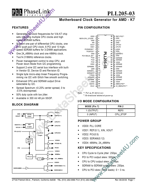
PIN CONFIGURATION e h
- Generates all clock frequencies for VIA K7 chip S sets requiring ta multiple CPU clocks and high speed a SDRAM buffers.
- Support one pair of differential CPU clocks, one .D 3.3V push-pull CPU clock, 6 PCI and 13 highw speed SDRAM buffers for 3-DIMM applications. w w- One 24_48MHz clock and one 48MHz clock.
- -
- -
- -
- - Two14.318MHz reference clocks. Power management control to stop CPU, and Power down Mode from I2C programming. Support 2-wire I2C serial bus interface with builtin Vendor ID, Device ID and Revision ID. Single byte micro-step linear Frequency Programming via I2C with Glitch free smooth switching. Enhanced CPU and SDRAM output Drive selectable by I2C. Spread Spectrum ± 0.25% center spread, 0 to -0.5% downspread. 50% duty cycle with low jitter. Available in 300 mil 48 pin SSOP.
BLOCK DIAGRAM
XIN XOUT
XTAL OSC
SDATA SCLK FS (0:3)-
I2C Logic
PLL1 SST m o .c U 4 t e e h S a t a .D w w w
8 9 41 40 39 38 37 36 35 34 33 32 31 30 29 28...