PhaseLink PLL205-16
The internal clocks are disabled and the VCO and the crystal are stopped. When input is Low, it will stop PCI(0:8) and PCI9_E.| Part No. | PLL205-16 |
|---|---|
| Datasheet | PLL205-16 Download |
| Manufacturer |  PhaseLink |
| Description | Programmable Clock Generator |
| Buy | Stock & Price |
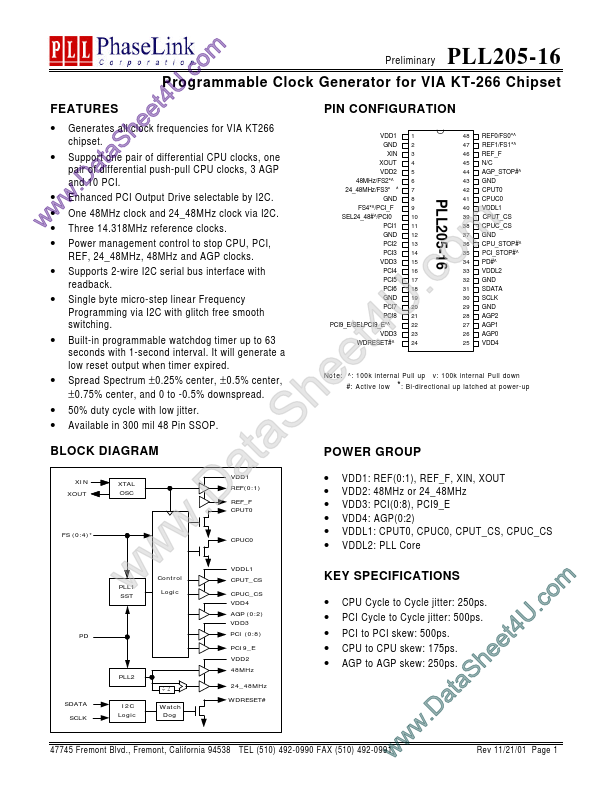
FEATURES
PIN CONFIGURATION e e frequencies for VIA KT266● Generates all clock h chipset. S a
● Support one t pair of differential CPU clocks, one pair of a differential push-pull CPU clocks, 3 AGP and D 10 PCI. .
● w Enhanced PCI Output Drive selectable by I2C.
●w One 48MHz clock and 24_48MHz clock via I2C. w● Three 14.318MHz reference clocks.
●
●
●
●
●
●
● Power management control to stop CPU, PCI, REF, 24_48MHz, 48MHz and AGP clocks. Supports 2-wire I2C serial bus interface with readback. Single byte micro-step linear Frequency Programming via I2C with glitch free smooth switching. Built-in programmable watchdog timer up to 63 seconds with 1-second interval. It will generate a low reset output when timer expired. Spread Spectrum ± 0.25% center, ± 0.5% center, ± 0.75% center, and 0 to -0.5% downspread. 50% duty cycle with low jitter. Available in 300 mil 48 Pin SSOP. BLOCK DIAGRAM XIN XOUT XTAL OSC FS (0:4)* PLL1 SST m o .c U 4 t e e h S a t a .D w w w 10 11 12 13 14 15 16 17 18 19 2...

