PhaseLink PLL602-10
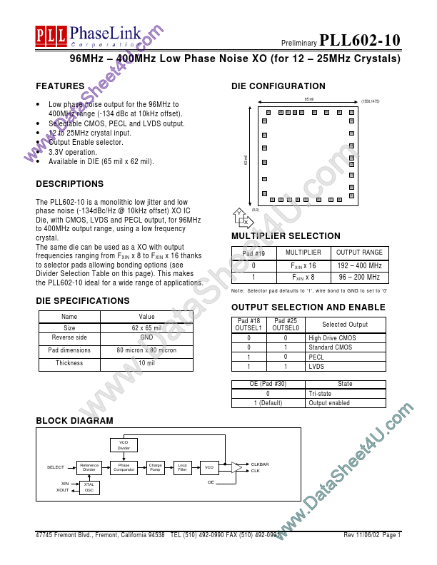
The PLL602-10 is a monolithic low jitter and low phase noise (-134dBc/Hz @ 10kHz offset) XO IC Die, with CMOS, LVDS and PECL output, for 96MHz to 400MHz output range, using a low frequency crystal. The same die can be used as a XO with output frequencies ranging from F XIN x 8 to F XIN x 16 thanks to selector pads allowing bonding options (see Divider Selection Table on this page). This makes the PLL602-10 ideal for a wide range of applications.| Part No. | PLL602-10 |
|---|---|
| Datasheet | PLL602-10 Download |
| Manufacturer |  PhaseLink |
| Description | Low Phase Noise XO |
| Buy | Stock & Price |
FEATURES
●●
●
●
●
● w 62 mil w w Low phase noise output for the 96MHz to 400MHz range (-134 dBc at 10kHz offset). Selectable CMOS, PECL and LVDS output. 12 to 25MHz crystal input. Output Enable selector. 3.3V operation. Available in DIE (65 mil x 62 mil). .D a ta Sh t e e 4U . m o c Preliminary PLL602-10 DIE CONFIGURATION 65 mil (1550,1475) 19 18 17 16 25 26 24 23 22 21 20 27 15 28 14 29 30 DESCRIPTIONS 31 1 2 3 4 5 Y X (0,0) MULTIPLIER SELECTION DIE SPECIFICATIONS Name Size Reverse side Pad dimensions Thickness Value 62 x 65 mil GND 80 micron x 80 micron BLOCK DIAGRAM VCO Divider w w w 10 mil .D Charge Pump t a S a e h 0 0 1 1 Pad #19 0 1 t e U 4 0 1 0 1 .c 6 m o 13 12 11 10 9 7 8 MULTIPLIER OUTPUT RANGE F XIN x 16 F XIN x 8 192 – 400 MHz 96 – 200 MHz Note: Selector pad defaults to ‘1’, wire bond to GND to set to ‘0’ OUTPUT SELECTION AND ENABLE Pad #18 OUTSEL1 Pad #25 OUTSEL0 Selected Output High Drive CMOS Standard CMOS PECL LVDS State Tri-state Output enabled OE (Pad #30) 0 1 (Defa...